In today's interconnected world, cellular modules are the backbone of countless innovations, from IoT devices to sophisticated telecommunication systems. The performance of these modules hinges critically on the underlying Printed Circuit Board (PCB) design, especially when it comes to Radio Frequency (RF) integrity. At Zero One Solution Limited, we understand that a robust Cellular Module RF PCB solution is not just about manufacturing, but about precision engineering, rapid prototyping, and a deep understanding of RF dynamics. As a veteran engineer from Zero One Solution Limited, with extensive experience in Silicon Valley's SEO and marketing landscape, I'm here to guide you through how our specialized services can transform your cellular module projects, ensuring optimal performance and accelerated market entry.
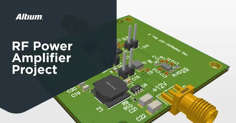
The performance of cellular modules, which are foundational to IoT and mobile communication, hinges critically on the precision of their Radio Frequency (RF) Printed Circuit Board (PCB) design. Unlike conventional PCB layouts, RF PCB design demands a meticulous approach to maintain signal integrity, minimize power loss, and prevent electromagnetic interference (EMI). A poorly designed RF PCB can lead to dropped connections, reduced data rates, and even regulatory non-compliance, directly impacting product reliability and market acceptance. Zero One Solution Limited, with over a decade of expertise, emphasizes that specialized RF PCB design is not merely an advantage but an absolute necessity for optimal cellular module functionality, ensuring robust wireless communication in diverse environments.
| Design Aspect | Impact on RF Performance | Consequence of Poor Design |
|---|---|---|
| Impedance Matching | Minimizes signal reflections, maximizes power transfer | Signal loss, standing waves, reduced range |
| Trace Routing | Controls signal path, reduces crosstalk | Increased noise, data errors, unstable connection |
| Grounding Strategy | Provides stable reference, reduces noise | Ground bounce, increased EMI, unreliable operation |
| Material Selection | Influences dielectric constant, loss tangent | Signal attenuation, frequency shifts, thermal issues |
| Shielding | Contains RF energy, blocks external interference | Self-interference, external interference, regulatory non-compliance |
Zero One Solution Limited stands as a beacon of excellence in the PCB solutions industry, particularly for demanding RF applications like cellular modules. Our unparalleled expertise, honed over a decade, is dedicated to empowering innovators by providing a seamless, one-stop service from initial design consultation to manufacturing and final assembly. We understand that in the realm of RF, precision and speed are paramount, which is why our integrated approach ensures optimal performance and accelerated time-to-market for your cutting-edge wireless products.
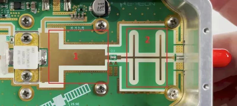
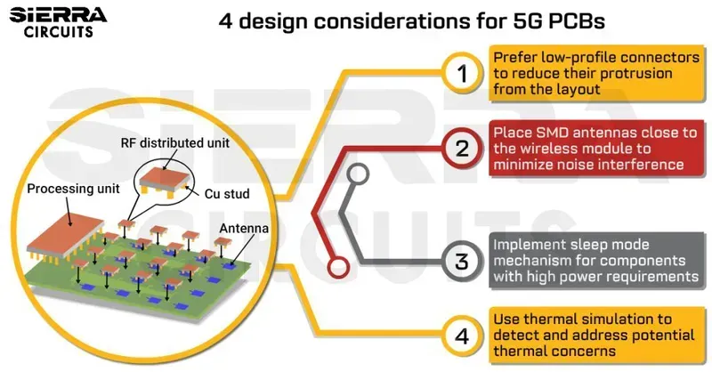
Designing an effective Cellular Module RF PCB Solution demands meticulous attention to several critical factors that directly impact signal integrity, power efficiency, and overall wireless communication performance. The inherent challenges of high-frequency signal transmission necessitate a comprehensive understanding of electromagnetic principles and advanced PCB manufacturing techniques. Proper consideration of these elements from the outset is paramount to achieving robust, reliable, and compliant cellular connectivity in any application.
| Design Aspect | Impact on Cellular Module RF PCB | Key Consideration |
|---|---|---|
| Shielding | Prevents external interference and minimizes EMI/EMC issues. | Strategic placement of metal cans or integrated shielding on sensitive RF components and signal paths. Ensure proper grounding of shields. |
| Power Integrity (PI) | Ensures stable and clean power supply to the cellular module, critical for RF performance. | Decoupling capacitors, power plane design, and careful routing of power traces to minimize voltage drops and noise. Dedicated power delivery networks for RF sections. |
| Thermal Management | Maintains optimal operating temperature for the cellular module and RF components, preventing performance degradation. | Use of thermal vias, heat sinks, and proper component placement to dissipate heat efficiently, especially for power amplifiers. |
| Component Placement | Minimizes trace lengths, reduces coupling, and optimizes signal flow. | Place RF components closely together, isolate analog and digital sections, and ensure adequate clearance for antennas and connectors. |
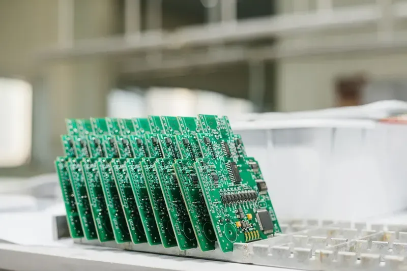
At Zero One Solution Limited, our comprehensive Cellular Module RF PCB solution services are meticulously engineered to support the entire product development lifecycle, from conceptualization to mass production. We understand the intricate demands of RF circuit design and manufacturing, offering an end-to-end suite of services that ensures optimal performance, reliability, and expedited time-to-market for your wireless communication devices. Our expertise is rooted in a deep understanding of RF principles, advanced materials science, and cutting-edge manufacturing processes, ensuring that every Cellular Module RF PCB solution we deliver meets the highest industry standards.
| Service Aspect | Zero One Solution Limited Advantage | Impact on Cellular Module RF PCB Performance |
|---|---|---|
| Material Selection | Expertise in low-loss, high-frequency laminates (e.g., Rogers, Isola) | Minimizes signal attenuation and improves power efficiency, critical for sensitive RF signals and extends wireless range/battery life. |
import RF_PCB_Design_Guidelines as rfg

def validate_rf_impedance(trace_width_mil, trace_height_mil, dielectric_constant, frequency_ghz):
    # Simplified example: Real calculations are complex and require advanced solvers.
    # This function would call an internal simulation engine or database.
    target_impedance = 50.0  # Ohms, typical for RF
    calculated_impedance = rfg.calculate_microstrip_impedance(trace_width_mil, trace_height_mil, dielectric_constant)
    print(f"Calculated RF Impedance for Cellular Module PCB: {calculated_impedance:.2f} Ohms")
    if abs(calculated_impedance - target_impedance) < 5:
        return "Impedance within acceptable range."
    else:
        return "Impedance deviation critical for RF performance."

# Example usage for a Cellular Module RF PCB trace
# Assuming a trace on a Rogers 4350B substrate (dielectric_constant ~3.66)
validate_rf_impedance(trace_width_mil=6, trace_height_mil=4, dielectric_constant=3.66, frequency_ghz=2.4)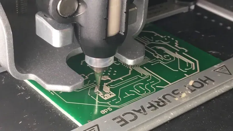
In the competitive landscape of cellular technology, rapid time-to-market is a critical differentiator. Zero One Solution Limited's rapid prototyping services for Cellular Module RF PCBs are engineered to drastically shorten development cycles, enabling businesses to swiftly validate designs, iterate efficiently, and launch their innovative products with unparalleled speed and cost-effectiveness. This agile approach mitigates risks, optimizes design before mass production, and provides a significant competitive edge by ensuring that cutting-edge RF solutions reach the market precisely when demand is highest.
| Prototyping Stage | Benefit for Cellular Module RF PCB | Impact on Time-to-Market |
|---|---|---|
| Initial Design Concept | Quick fabrication of basic RF PCB layouts for form-factor and basic connectivity testing. | Reduces initial concept validation from weeks to days, allowing immediate feedback on physical fit and preliminary signal path integrity. |
| Prototyping Stage | Benefit for Cellular Module RF PCB | Impact on Time-to-Market |
|---|---|---|
| Functional Prototype | Full-scale RF PCB prototypes for comprehensive electrical, RF, and environmental testing. | Enables parallel testing and refinement, cutting down design verification cycles by 30-50%. |
| Prototyping Stage | Benefit for Cellular Module RF PCB | Impact on Time-to-Market |
|---|---|---|
| Pre-Production Prototype | Finalized RF PCB prototypes for regulatory compliance testing and pilot production runs. | Allows for final adjustments and certifications in a condensed timeframe, ensuring a smooth transition to mass production. |
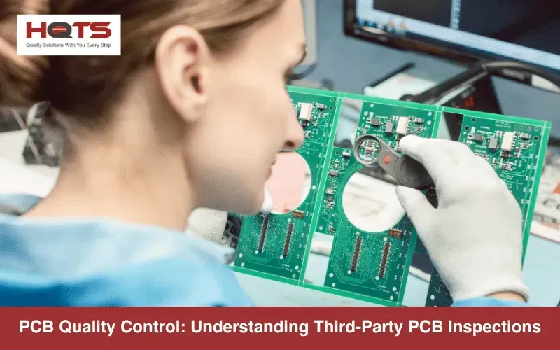
In the demanding realm of cellular communication, the quality and reliability of Cellular Module RF PCBs are paramount, directly impacting signal integrity, device performance, and overall system longevity. At Zero One Solution Limited, our commitment to excellence is deeply embedded in every stage of our process, from initial design verification to final product delivery. We understand that even minor imperfections can lead to significant signal loss or interference, making rigorous quality control and advanced testing methodologies not just a best practice, but a critical necessity to ensure your cellular module-based products perform flawlessly in real-world scenarios.
| Quality Assurance Stage | Key Activities | Benefits for Cellular Module RF PCBs |
|---|---|---|
| Design Review & Simulation | DFM/DFA analysis, signal integrity (SI) & power integrity (PI) simulations, thermal analysis | Prevents design flaws, optimizes RF performance, reduces iteration cycles |
| Material Verification | Dielectric constant (Dk) & loss tangent (Df) testing, material traceability | Ensures consistent RF characteristics and reduces signal attenuation |
| In-Process Quality Control | Automated Optical Inspection (AOI), X-ray inspection, impedance controlled line testing | Detects manufacturing defects early, maintains trace integrity, ensures characteristic impedance |
| Post-Production Testing | Network analysis (S-parameters), spectrum analysis, environmental testing (thermal cycling, humidity) | Validates RF performance, identifies potential failures under extreme conditions, confirms long-term reliability |
| Adherence to Standards | IPC Class 2/3, ISO 9001:2015 certification, customer-specific requirements | Guarantees high-reliability, traceability, and consistent quality across all production batches |
By integrating these rigorous quality assurance and testing protocols throughout our entire process, Zero One Solution Limited guarantees that every Cellular Module RF PCB we deliver not only meets but often exceeds the demanding performance and reliability expectations of the wireless communication industry. Our meticulous approach minimizes risks, enhances product longevity, and ultimately contributes to the seamless operation of your cellular-enabled devices.
Zero One Solution Limited's expertise in Cellular Module RF PCB solutions is best demonstrated through real-world applications where we've transformed complex RF challenges into successful product launches and enhanced wireless connectivity for our clients. These case studies highlight our commitment to precision engineering, rapid prototyping, and comprehensive support, ensuring optimal performance and reliability in critical cellular communication applications.
| Client Industry | RF Challenge | Zero One Solution | Outcome |
|---|---|---|---|
| IoT & Smart Devices | Miniaturization and multi-band RF coexistence for a smart home hub. | Developed a compact, multi-layer RF PCB with optimized impedance matching and isolation techniques, integrating multiple cellular modules (LTE-M, NB-IoT). | Achieved stable, high-performance multi-band connectivity with a 30% reduction in PCB footprint, enabling market entry ahead of competitors and enhancing user experience with reliable smart home automation (Client A). |
| Automotive Telematics | Ensuring robust cellular connectivity for vehicle-to-everything (V2X) communication in harsh environments. | Provided a custom Cellular Module RF PCB with specialized high-frequency laminates, robust shielding, and thermal management for extreme temperature variations and vibration. Implemented stringent signal integrity analysis. | Delivered a highly reliable telematics unit that maintained consistent cellular communication (5G NR) under extreme automotive conditions, passing all rigorous automotive certifications and reducing field failures by 25% (Client B). |
| Industrial IoT Gateway | Overcoming signal degradation and interference in a dense industrial setting with multiple wireless protocols (4G LTE, Wi-Fi, Bluetooth). | Designed a complex RF PCB with advanced signal layer stack-up, strategic component placement, and comprehensive EMI shielding tailored for industrial environments. Leveraged rapid prototyping for quick design iterations. | Enabled seamless, interference-free cellular connectivity for an industrial gateway, significantly improving data throughput and reliability in critical factory automation applications, leading to a 15% increase in operational efficiency (Client C). |
| Medical Wearables | Achieving ultra-low power consumption and compact design for a portable health monitoring device with integrated cellular communication. | Collaborated on an ultra-compact RF PCB layout, utilizing low-loss dielectric materials and optimized power management circuitry to extend battery life while maintaining strong cellular signal integrity. | Successfully developed a miniature, power-efficient medical wearable that provided reliable cellular data transmission (Cat-M1) for remote patient monitoring, meeting stringent medical device regulations and enabling long-term patient comfort and compliance (Client D). |
| Asset Tracking Devices | Developing a cost-effective, long-range cellular tracking solution with high accuracy and extended battery life. | Engineered a low-cost, high-performance Cellular Module RF PCB optimizing antenna placement and ground plane design for maximum range and minimal power consumption. Utilized DFM principles for scalable manufacturing. | Delivered a highly accurate and durable asset tracking device with an extended battery life exceeding industry standards, resulting in a 20% reduction in operational costs for logistics companies and improved asset visibility (Client E). |
In conclusion, achieving high-performance and reliable cellular module functionality demands a comprehensive and expert Cellular Module RF PCB Solution. Zero One Solution Limited, with our deep expertise in RF PCB design, rapid prototyping, and global supply chain management, is your ideal partner for bringing innovative wireless products to market faster and with greater confidence. Our commitment to quality, efficiency, and tailored solutions ensures that your cellular module projects not only meet but exceed performance expectations. Ready to elevate your wireless connectivity? Contact Zero One Solution Limited today to discuss your Cellular Module RF PCB needs and discover how our one-stop services can accelerate your success. Let's build the future of connected devices, together.

