In today's technology-driven world, circuit board assembly forms the bedrock of nearly every electronic device we rely on. From smartphones to complex medical equipment, the precision and quality of PCB assembly are paramount. This article delves into the intricacies of circuit board assembly, exploring key steps, component types, and crucial aspects that guarantee high-performance and reliable electronic products. We aim to demystify the process and offer actionable insights for both newcomers and seasoned professionals.
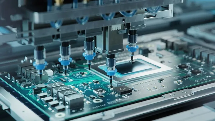
Circuit Board Assembly (PCBA) refers to the process of populating a bare Printed Circuit Board (PCB) with electronic components, creating a functional electronic module. This critical step in electronics manufacturing transforms a passive board into an active component capable of performing specific functions. Unlike a bare PCB, which is simply a substrate with conductive pathways, a PCBA includes all the necessary electronic components, such as resistors, capacitors, integrated circuits, and connectors, soldered onto the board. The PCBA process is fundamental to the creation of virtually all electronic devices.
The PCBA process is not a monolithic task, but rather a multi-stage operation involving careful preparation, precision placement, and meticulous soldering. These stages are sequenced to ensure that every component is accurately placed and securely attached, thereby guaranteeing the performance and reliability of the final product. The quality of the PCBA directly impacts the functionality of the overall system, making it a crucial aspect of the manufacturing process.
| Feature | Bare PCB | PCBA |
|---|---|---|
| Definition | A substrate with conductive tracks | A populated PCB with electronic components |
| Functionality | Passive, does not perform any electronic function | Active, performs intended electronic function |
| Components | No electronic components | Includes resistors, capacitors, ICs, etc. |
| Manufacturing Stage | Initial stage of circuit board production | Later stage, assembling components onto the PCB |
| Use Case | Used as a base for electronic circuits | Used in electronic devices as functional module |
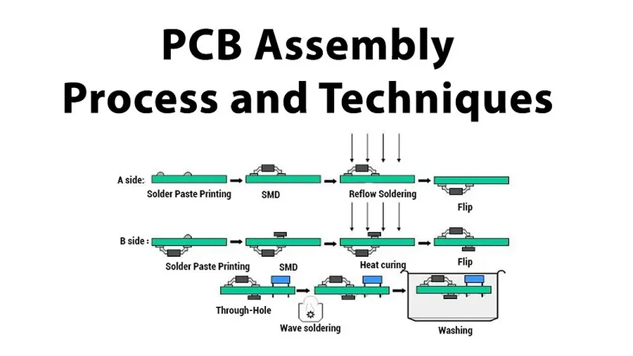
The Printed Circuit Board Assembly (PCBA) process is a multi-stage operation that transforms a bare PCB into a functional electronic component. Each step is critical, demanding precision and adherence to specifications to ensure the final product's reliability and performance. The process encompasses a range of techniques, from applying solder paste to rigorous testing protocols.
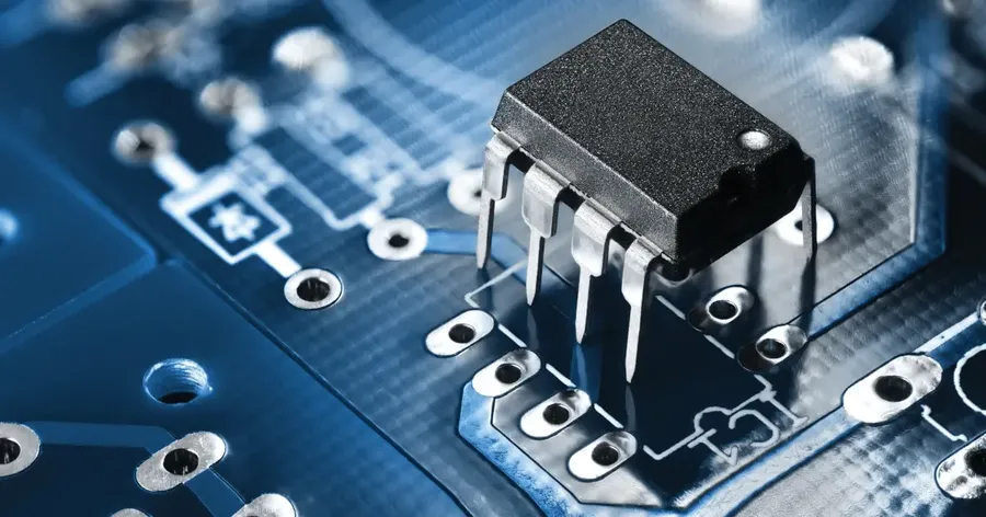
Surface Mount Technology (SMT) and Through-Hole Assembly are the two primary methods for attaching electronic components to a printed circuit board (PCB). SMT involves mounting components directly onto the surface of the PCB, while through-hole technology requires inserting component leads into drilled holes on the board. The choice between these methods depends on factors like component type, production volume, and required robustness.
| Feature | Surface Mount Technology (SMT) | Through-Hole Assembly |
|---|---|---|
| Component Mounting | Components are mounted directly onto the PCB surface. | Components are inserted through holes in the PCB. |
| Component Size | Suitable for small, miniaturized components. | Suitable for larger, more robust components. |
| Component Lead Style | Components have leads designed for surface mounting (e.g., pads, gull-wing, J-lead) | Components have leads that extend through the PCB (e.g., axial, radial) |
| Assembly Automation | Highly suitable for automated pick-and-place machines and reflow soldering. | Requires manual assembly or specialized wave soldering processes. |
| Manufacturing Density | Allows for higher component density due to smaller footprint. | Limited by the size and spacing of through-hole components. |
| Cost | Generally lower per unit cost for high-volume production. | Generally higher cost for high-volume production, and more expensive for low volumes. |
| Mechanical Strength | More susceptible to mechanical stress if not correctly assembled. | Provides stronger mechanical connection to the PCB. |
| Applications | Dominant method for most modern electronic devices, mobile phones, consumer electronics. | Used for robust, high-power, or high-stress applications, such as connectors, transformers, electrolytic capacitors. |
The selection between SMT and through-hole is not always a binary choice. It is common to see hybrid designs that incorporate both SMT and through-hole components. Hybrid assembly allows leveraging of the advantages of each method, such as high-density SMT components for general circuitry with robust through-hole components for connectors and larger power devices. Understanding the benefits and drawbacks of each method ensures the most efficient and cost-effective circuit board assembly process.
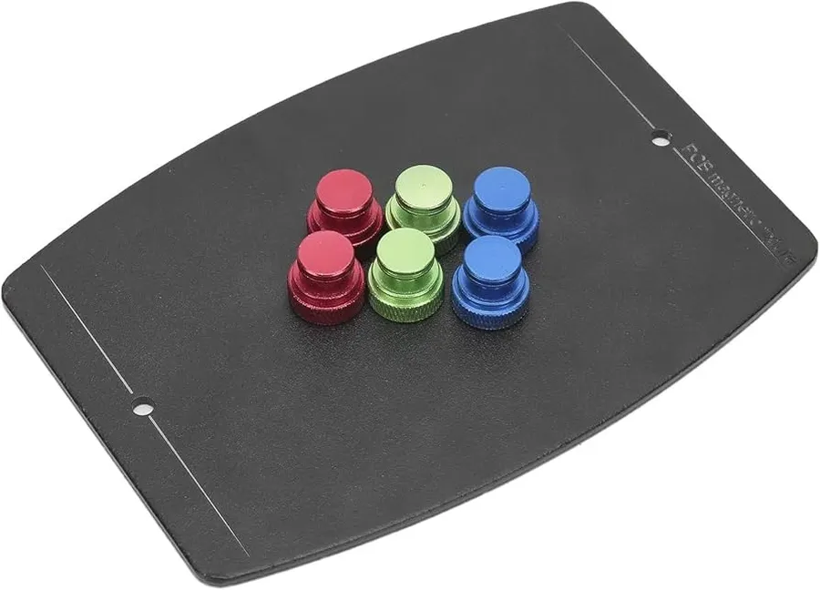
The precision and reliability of circuit board assembly (PCBA) are heavily dependent on the tools and equipment employed. This section outlines the essential tools necessary for both prototyping and high-volume production, ensuring consistent and quality results.
| Equipment Category | Specific Tools/Equipment | Purpose | Prototyping Use | Production Use |
|---|---|---|---|---|
| Solder Paste Application | Solder Paste Stencil | Precisely applies solder paste to PCB pads | Manual stencil or basic printer | Automated stencil printer |
| Component Placement | Pick-and-Place Machine | Accurately places components onto the PCB | Manual placement or basic pick-and-place | High-speed, automated pick-and-place |
| Soldering | Reflow Oven | Melts solder paste to form electrical connections | Small, basic reflow oven | Larger batch or continuous reflow oven |
| Soldering | Wave Soldering Machine | Solders through-hole components | Generally not used for prototyping | Used for through-hole components in high-volume production |
| Soldering | Soldering Iron/Station | Manual soldering of components | Essential for rework and minor assembly | Used for manual rework and specialized soldering |
| Cleaning | Ultrasonic Cleaner or Cleaning Solution | Removes flux residue after soldering | Small ultrasonic cleaner | Automated cleaning system |
| Inspection | Microscope/Magnifying Glass | Visually inspect solder joints and component placement | Essential for initial inspection | Used for QA and process monitoring |
| Inspection | Automated Optical Inspection (AOI) System | Automated inspection of PCBs for defects | Not essential for prototyping | Crucial for high-volume quality control |
| Testing | Multimeter | Measures electrical parameters to verify connectivity | Used for basic circuit checks | Used for diagnostic testing |
| Testing | In-Circuit Tester (ICT) | Tests assembled boards for correct operation | Not often used in prototyping | Essential for high-volume production testing |
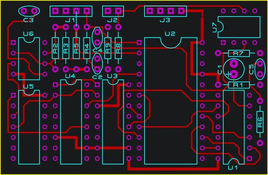
Design for Assembly (DFA) is a crucial methodology in circuit board assembly that focuses on optimizing a PCB's design to streamline the manufacturing process, thereby reducing assembly time, errors, and overall costs. Effective DFA implementation ensures that a design is not just functional but also readily manufacturable. It involves considering the entire assembly process during the design phase, paying close attention to component placement, orientation, and the specific requirements of automated assembly equipment.
Key aspects of DFA include:
Following DFA best practices offers several advantages:
Cost-saving tips through DFA include: minimizing the number of different component types, standardizing footprints and component values, and optimizing the board size for efficient panelization. By incorporating DFA principles into the PCB design process, manufacturers can substantially improve the overall quality and efficiency of circuit board assembly.
The cost of circuit board assembly (PCBA) is influenced by a multitude of interconnected factors, encompassing not only the raw materials but also the complexity of the design, the chosen assembly methods, and the scale of production. Understanding these cost drivers is crucial for effective budget planning and cost optimization in electronics manufacturing.
| Cost Factor | Description | Impact on Cost |
|---|---|---|
| Component Costs | Price of individual electronic components (resistors, capacitors, ICs, etc.) used on the PCB. | Directly proportional to the total cost; higher-priced components increase overall PCBA cost. |
| Assembly Method | The technology used for component mounting (SMT, through-hole, mixed). | SMT is generally more cost-effective for mass production, while through-hole can be more expensive due to manual processes. |
| Production Volume | The number of circuit boards being assembled. | Larger volumes often lead to reduced per-unit costs due to economies of scale; prototype volumes can be more expensive. |
| PCB Complexity | Number of layers, component density, board size and shape, and design rules. | More complex designs with fine-pitch components and multi-layer boards increase assembly difficulty and costs. |
| Turnaround Time | The time required to complete the assembly process. | Express or expedited assembly typically incurs higher costs due to overtime and rush handling. |
| Testing Requirements | Level of quality control checks including visual inspection, in-circuit testing, and functional tests. | Stringent testing protocols will increase costs but ensures higher reliability. Functional tests are most expensive. |
| Material Sourcing | Cost of procuring components and the printed circuit board itself (from different suppliers, bulk vs. small quantities, etc.) | Higher cost components or the boards themselves may raise overall assembly costs. |
| Engineering Preparation | Time spent on design checks, generating assembly files, and preparing for production. | Upfront non-recurring engineering (NRE) costs should be considered; more intensive checks increase costs. |
Strategies for managing and optimizing PCBA costs include careful component selection, choosing appropriate assembly techniques based on volume, simplifying designs where possible without compromising performance, planning for adequate production time and lead times to avoid rush orders, and thoroughly optimizing PCB designs for manufacturability to reduce NRE costs. Early engagement with an assembly service provider to leverage their expertise can also reveal design optimizations that significantly impact final costs. Furthermore, consider the overall impact of testing methodologies, with functional testing representing a higher cost due to the level of testing rigor.
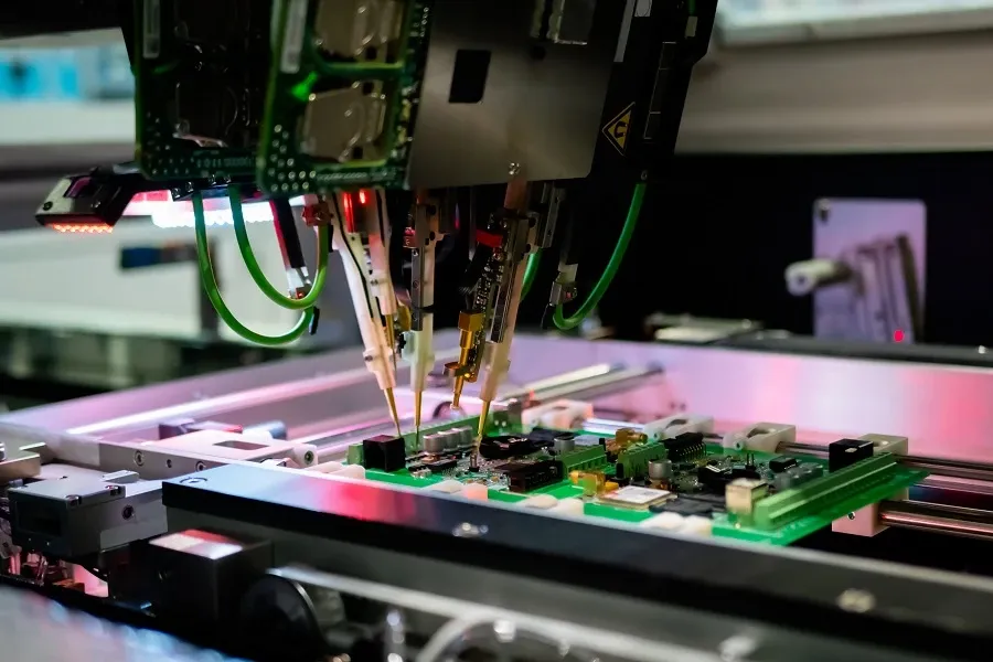
Rigorous quality control and testing are paramount in ensuring the reliability and functionality of a Printed Circuit Board Assembly (PCBA). These processes identify defects early, preventing costly failures in the final product. Comprehensive testing encompasses various methods, each targeting different potential issues.
| Testing Method | Description | Purpose |
|---|---|---|
| Visual Inspection | Manual or automated examination of the PCB for visible defects such as solder bridges, misaligned components, and incorrect polarity. | Detects gross physical defects and assembly errors. |
| In-Circuit Testing (ICT) | Uses a bed-of-nails fixture to access test points on the PCB and verify the electrical performance of individual components and circuits. | Verifies proper component placement, orientation, and electrical functionality of the PCB. |
| Automated Optical Inspection (AOI) | Utilizes high-resolution cameras and image processing algorithms to detect surface defects such as incorrect component placement, solder joint issues, and missing components. | Provides consistent and accurate inspection. |
| Functional Testing | Simulates the real-world operating conditions of the PCB to verify if it meets its design specifications. | Tests the performance of the PCBA within its application. |
| X-Ray Inspection | Uses X-ray imaging to detect hidden defects, such as voids in solder joints or misaligned BGA (Ball Grid Array) components. | Detects defects that cannot be observed with visual inspection or AOI. |
The selection of testing methods depends on several factors, including the complexity of the PCBA, the volume of production, and the criticality of the application. Often, a combination of testing methods is employed to achieve the highest level of reliability. These stringent quality control and testing protocols are essential to ensuring the delivery of high-quality, fully functional PCBAs.
This section addresses common queries regarding circuit board assembly (PCBA), providing clear and concise answers to help clarify the distinctions, processes, and cost considerations involved in PCBA.
Selecting the right PCB assembly service provider is crucial for ensuring the quality, reliability, and cost-effectiveness of your electronic products. This section details the key factors to consider when making this important decision, encompassing both local and overseas options.
Circuit board assembly is a complex but critical process in electronics manufacturing. By understanding the different steps, technologies, and best practices discussed, it's possible to achieve high-quality and reliable PCBA. Whether you're a design engineer or a business looking to produce electronics, understanding the full life cycle of circuit board assembly, from design to testing, is vital for success. Embracing precision, quality control, and working with experienced assembly partners guarantees that your electronic devices perform effectively. With the rapid pace of technological advancement, a deep comprehension of PCBA becomes evermore crucial for future innovation.

