Design Your Dream: A Comprehensive Guide to Custom PCBs
2025.01.25
In our increasingly interconnected world, custom PCBs are the unsung heroes powering countless devices. From the simplest Arduino project to advanced aerospace technology, the ability to design a custom PCB allows for unparalleled flexibility and optimization. This article will explore the world of custom PCBs, covering everything from initial design considerations to cost factors, empowering you with the knowledge to bring your electronic projects to life, with custom PCB at the heart of the process.
Understanding Custom PCBs: What Makes Them Special?
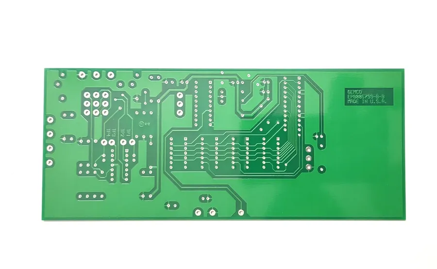
Custom PCB
Custom Printed Circuit Boards (PCBs) are specifically designed and manufactured to meet the unique requirements of a particular application, offering significant advantages over standard, off-the-shelf PCBs. These advantages stem from tailored design parameters, optimized performance characteristics, and the ability to address specific functional needs.
The core benefits of opting for custom PCBs are:
Design Flexibility Custom PCBs allow for unparalleled design flexibility. Engineers can create boards with specific shapes, sizes, and layouts to perfectly fit within their product enclosures. This freedom extends to the placement of components, trace routing, and the integration of unique features.
Performance Optimization By customizing PCB design, performance can be optimized for specific needs. This includes adjusting trace impedance for signal integrity, strategically placing components to minimize interference, and selecting materials suitable for specific electrical and thermal requirements. Consequently, custom PCBs can offer higher performance and reliability over generic solutions.
Meeting Unique Application Needs Many applications have unique requirements that cannot be met by off-the-shelf PCBs. Custom PCBs can be tailored to accommodate these requirements, including specific connector types, specialized component footprints, or unique power delivery systems. This adaptability makes them essential for innovative product development.
Size and Space Constraints In many modern applications, especially in portable electronics, space is at a premium. Custom PCBs can be designed to fit into very tight spaces, which is often not possible with off-the-shelf options. Their ability to be tailored to specific size and form factor requirements allows for compact and efficient product designs.
Integration of Advanced Technologies Custom PCBs facilitate the integration of advanced technologies that may be difficult or impossible to implement on standard boards. This includes high-density interconnects (HDI), complex multi-layer structures, and the integration of specific materials that offer superior performance characteristics (e.g., thermal management or higher frequency capabilities).
The Custom PCB Design Process: A Step-by-Step Guide
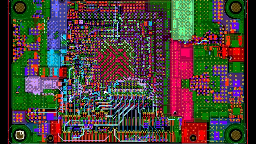
PCB Design Software
The journey of creating a custom Printed Circuit Board (PCB) involves a meticulous design process, transforming an abstract idea into a tangible electronic component. This section details the crucial phases from initial schematic capture to the generation of manufacturing files, providing insights into best practices and essential software tools.
Schematic Capture This initial stage involves creating a circuit diagram representing the electronic connections and components of your intended PCB. It's essential to select appropriate components from a library and link them according to the functional requirements. This stage is crucial for defining the electrical behavior of the circuit. The schematic is a blueprint, it should be accurate, and clear, as it will guide all further steps.
PCB Layout Design Building upon the schematic, the layout process translates the circuit diagram into a physical representation. This involves positioning components, defining the copper tracks or traces to make connections, and determining the layer stack up of the board. Consideration should be given to signal integrity, thermal management, and manufacturability. Factors such as trace width and impedance matching should be carefully planned.
Gerber File Generation Gerber files are the standard format used in PCB manufacturing, which represent each layer of the PCB as a vector based image. These are essential to communicate your design to the manufacturer. The process involves exporting all necessary manufacturing information, including copper layers, solder mask, silkscreen, and drill information. Ensuring correct and complete Gerber files is paramount for accurate PCB production.
Design Rule Checks (DRC) Before generating the Gerber files, performing a thorough DRC is crucial. DRC checks your design against predefined manufacturing rules, verifying sufficient clearances, trace widths, and other parameters to ensure manufacturability and signal integrity. This helps to reduce potential errors and cost during the production phase.
Several Electronic Design Automation (EDA) software tools facilitate the design process, each with its strengths and user interface. Popular tools include Altium Designer, KiCad, Eagle, and OrCAD, with KiCad being an open-source option. Choosing the right software depends on project complexity, budget and individual preference. Regardless of the chosen tool, proficiency in its operation is essential for successful PCB design. Additionally, some online tools can offer basic features for simple designs.
Design Parameter
Description
Impact
Layer Count
The number of copper layers in the PCB.
Complexity, cost, and signal integrity. More layers allow for more complex routing and better signal characteristics, but at a higher cost.
Track Width and Spacing
Dimensions of conductive traces and the space between them.
Impacts current-carrying capacity and signal isolation. Accurate calculation prevents overheating or signal interference.
Via Size and Type
Dimension and type of vias used to connect layers
Affects manufacturability, signal integrity, and impedance. Careful selection is vital for proper electrical performance.
Component Placement
Physical location and orientation of components on the board
Critical for routing, thermal management and manufacturability. Strategic placement reduces signal noise and improves the overall PCB performance.
Material Selection
Choice of substrate material (e.g. FR4, Aluminum)
Directly impacts temperature resistance, signal properties, and cost. Different materials are suitable for different operational requirements and environmental conditions.
Selecting the Right Custom PCB Manufacturer
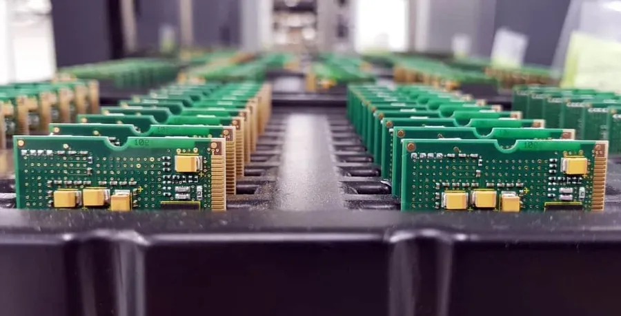
PCB Manufacturing Facility
Choosing the correct custom PCB manufacturer is critical to the success of any electronics project. This decision significantly influences the final product's quality, cost, and timeline. It's essential to evaluate potential partners based on several key factors to ensure they align with your project requirements and specifications.
Here is a structured breakdown of the essential criteria:
Turnaround Time Assess the manufacturer's lead times for both prototype and production runs. Faster turnaround times can be crucial for rapid prototyping, while predictable timelines are necessary for production planning. Consider that lead times can vary significantly depending on the PCB's complexity and the manufacturer's current workload. Some manufacturers offer expedited services for an additional cost, which might be beneficial for urgent projects.
Cost Evaluate the total cost, encompassing tooling, per-unit prices, and potential shipping fees. The lowest price may not be the best value if quality or reliability are compromised. Understand that pricing is influenced by board size, layer count, material selection, and finish options. Requesting multiple quotes is recommended to secure a competitive rate without sacrificing project requirements.
Material Options Ensure that the manufacturer offers the specific materials you require for your application. Common materials include FR-4, aluminum-backed PCBs for thermal management, and flexible substrates for wearable applications. Material choice impacts signal integrity, thermal performance, and mechanical resilience, directly influencing product functionality.
Surface Finish Options Verify the availability of various surface finishes like HASL, ENIG, or immersion silver, each with distinct advantages in terms of solderability, cost, and environmental impact. The correct surface finish protects copper traces from oxidation and improves the lifespan of the PCB.
Special Features and Capabilities Confirm if the manufacturer supports any special requirements such as blind and buried vias, controlled impedance traces, or via-in-pad technology. High-density interconnects and specific design features often necessitate advanced manufacturing capabilities, so ensure the manufacturer is suitably equipped.
Production Volume Capabilities Check if the manufacturer can meet your anticipated production needs, from initial prototypes to high-volume manufacturing runs. Selecting a scalable manufacturer ensures seamless transitions between different production stages and prevents delays. Manufacturers who have different production lines for prototype and production runs can streamline the process.
Geographical Location and Support Consider the manufacturer's location in relation to your company for potential logistical benefits. Communication and timezone compatibility are also important factors for efficient communication and rapid issue resolution. Local manufacturers might be suitable for smaller projects, and international ones might offer more cost-effective solutions for large-volume runs.
Quality Assurance and Certifications Inquire about the manufacturer’s quality control processes and certifications (e.g., ISO 9001, IPC standards). Stringent quality control directly impacts reliability of the PCBs. Reputable manufacturers should also have testing procedures in place, such as electrical testing and visual inspection, to ensure high-quality output.
While some manufacturers specialize in rapid prototyping and short runs, others excel in high-volume production. Understanding your specific needs will help you prioritize the selection criteria and choose a manufacturer that is the best fit for your project.
Selecting a PCB manufacturing partner involves not only meeting immediate technical needs but also building a reliable supply chain for future projects.
Cost Factors of Custom PCB Manufacturing
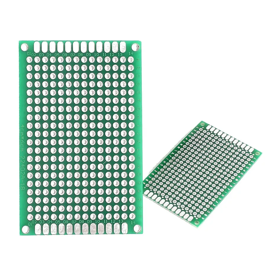
PCB Prototypes
Understanding the cost drivers in custom PCB manufacturing is crucial for optimizing both budget and design. Several factors contribute to the overall price, and a thorough grasp of these elements allows for informed decision-making, ensuring that financial considerations do not compromise the quality or performance of the final product.
Cost Factor
Description
Impact on Cost
Optimization Strategies
Board Size
The physical dimensions of the PCB.
Larger boards require more material, increasing costs.
Optimize board size by using efficient layouts and compact component placements.
Layer Count
The number of copper layers within the PCB.
More layers increase complexity, processing time, and material usage.
Use the minimum number of layers required for your design, possibly using design rules that allow for fewer layers.
Material Type
The base material used for PCB fabrication (e.g., FR-4, Aluminum, Flexible).
Advanced or high performance materials (Aluminum, Flexible) have higher costs than standard materials like FR-4
Choose a material that balances performance with cost requirements; FR-4 is generally the most cost-effective unless the application needs specific material properties.
Drilling
The number, size, and precision of holes drilled in the PCB.
More holes, vias, small hole sizes, tight tolerances, and microvias lead to higher costs.
Use larger via sizes if possible and optimize drilling parameters by avoiding extremely small drill sizes.
Surface Finish
Type of coating applied to the PCB to protect copper and ensure solderability (e.g., HASL, ENIG, Immersion Tin).
More advanced finishes like ENIG are more expensive than HASL.
Choose the surface finish that balances performance needs and costs; HASL (Hot Air Solder Leveling) is generally the most cost effective.
Optional Additions
Special features like impedance control, controlled depth milling, and blind/buried vias.
These features require more complex manufacturing processes increasing costs.
Only include these features when necessary and choose manufacturers with specialized options.
Production Volume
The quantity of PCBs manufactured in a single run.
Larger production volumes lead to lower per-unit costs due to economies of scale.
Consider batching small orders to achieve better volume discounts, while ensuring that the storage of PCBs is viable.
Selecting the right manufacturer can drastically affect the final cost. Manufacturers with specialized equipment for small hole sizes or advanced surface finishes may charge a premium, whereas those focused on higher volumes of simpler designs may offer more competitive pricing. It’s crucial to assess a manufacturer's capabilities, volume capacity, and location to make a cost-effective choice based on your specific project needs. Strategies for minimizing expenses involve a combination of design choices and strategic sourcing.
PCB Materials and Their Impact on Performance
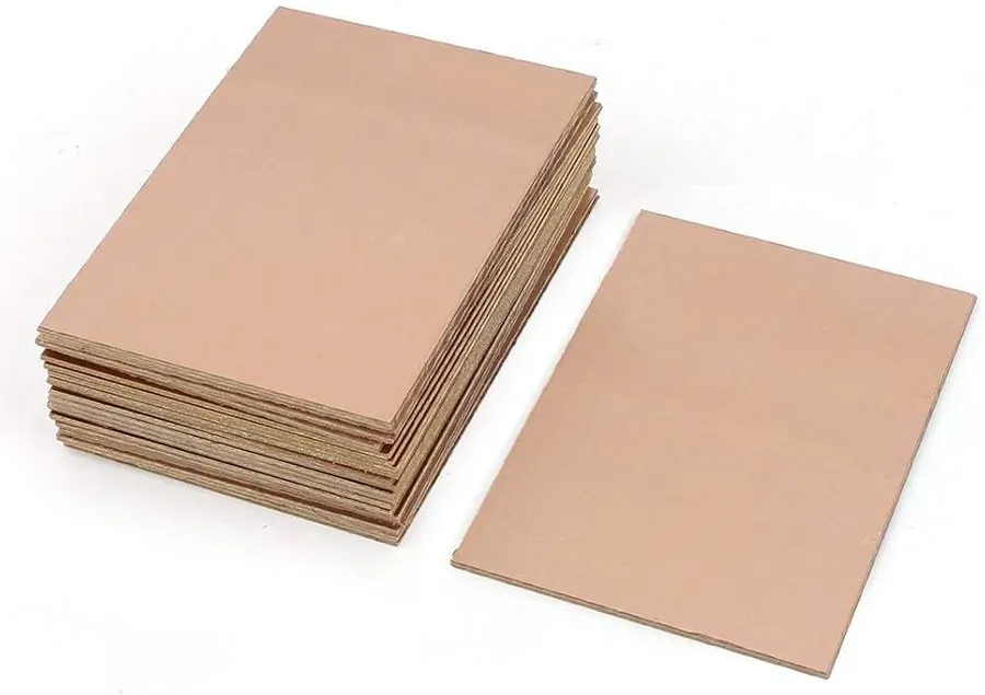
PCB Material
The selection of materials for a Printed Circuit Board (PCB) is paramount, significantly influencing its performance across diverse applications. Material properties directly impact signal integrity, thermal management, mechanical stability, and the overall longevity of the PCB. Understanding these impacts is crucial for optimizing PCB design for specific operational environments and requirements.
Material
Description
Key Characteristics
Typical Applications
FR-4
The most widely used PCB substrate material; a composite of woven fiberglass cloth with an epoxy resin binder.
Good mechanical strength, moderate electrical properties, relatively low cost. Offers a balance between performance and cost-effectiveness.
General electronics, consumer products, most standard PCB applications where extremely high performance or specialized thermal requirements are not critical.
Aluminum
Often used as a metal core PCB substrate for enhanced thermal dissipation.
Excellent thermal conductivity, good mechanical strength, ideal for applications generating significant heat.
LED lighting, power electronics, high-power applications where heat dissipation is crucial.
Flexible PCBs (Polyimide, Polyester)
Polyimide or polyester based materials for flexible circuit boards.
High flexibility, lightweight, excellent electrical and mechanical properties. Supports complex designs and dynamic bending.
Wearable devices, medical devices, automotive applications, consumer electronics requiring flexibility and compact size.
Rogers Materials
Specialized high-frequency laminates with proprietary filler systems
Superior high-frequency performance, excellent thermal properties, low loss tangent. Suited to high-speed digital and RF applications.
High-speed digital circuits, RF and microwave applications, telecommunications, aerospace and defense.
Signal Integrity The dielectric constant and loss tangent of the material affect signal transmission speed and signal losses, especially at higher frequencies. Materials with lower dielectric constants enable faster signal transmission, whereas lower loss tangents reduce signal degradation over long traces. Rogers materials are known for superior high-frequency performance.
Temperature Resistance Different materials exhibit varying degrees of temperature resistance. FR-4 is suitable for standard operating temperatures but may not be sufficient for high-temperature environments. Aluminum PCBs are used where heat dissipation is important, and some specialized materials offer even better performance. Polyimide can be used for flexible PCBs, providing a stable structure even at high temperatures.
Mechanical Properties The mechanical strength and flexibility of PCB materials impact the physical durability and design possibilities of the board. FR-4 is known for its rigidity, while flexible PCBs are essential for applications with bending requirements. The material's strength can also impact how well the PCB withstands the mechanical stresses during operation.
Cost Considerations The cost of different PCB materials varies significantly. FR-4 is generally the most cost-effective, making it ideal for general purpose applications. Specialized materials like Rogers or Aluminum will increase the overall cost of the PCB, but may be necessary for specific requirements.
Custom PCB Assembly: The Next Step
PCB Assembly Process
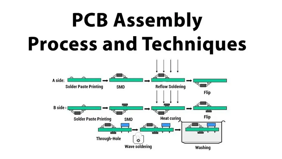
Custom PCB assembly is the crucial phase that follows manufacturing, transforming a bare circuit board into a functional electronic device. This process involves the precise placement and soldering of electronic components onto the fabricated PCB, completing the circuit and enabling its intended operation. Often, PCB assembly services are bundled with manufacturing to provide a seamless, end-to-end solution.
Surface Mount Technology (SMT) The most common method for assembling PCBs, SMT involves placing components directly onto the surface of the board and soldering them in place. This is a highly automated process suitable for large-volume production and small, intricate components.
Through-Hole Technology (THT) THT involves inserting components with leads through holes on the PCB and soldering them on the opposite side. While less common than SMT for modern PCBs, it is still used for larger and more robust components.
Mixed Assembly Many PCBs require a combination of SMT and THT assembly, depending on the type of components used in the design. This requires a more flexible assembly process with both SMT and THT capabilities.
Service
Description
Typical Use Cases
Full Turnkey Assembly
The manufacturer handles all aspects from component sourcing to final assembly. This provides a convenient solution, but typically involves higher overall costs.
Projects needing a complete service and where managing component sourcing and assembly in-house is not feasible.
Partial Turnkey Assembly
The customer provides some of the components and the manufacturer handles the remainder of the assembly process. This allows some control over costs or specific brands.
Projects that need a specific type or brand of component but want to outsource other parts of the process.
Consigned Assembly
The customer provides all components and the manufacturer is responsible solely for assembly. Lower cost than other options but involves customer managing components.
Projects where the customer has existing stock of components or specific requirements.
Frequently Asked Questions About Custom PCBs
This section addresses common inquiries regarding custom PCBs, encompassing various aspects from design tools to manufacturing considerations. This aims to provide clear and concise answers to assist those venturing into custom PCB development.
What software is commonly used for designing custom PCBs? Several software options are available, catering to different skill levels and project complexities. Popular choices include Altium Designer, Eagle PCB, KiCad, and OrCAD. KiCad is a robust open-source option, while Altium Designer is a high-end, industry-standard tool. The selection often depends on your budget, project complexity, and specific design requirements.
How long does it typically take to manufacture custom PCBs? Manufacturing time for custom PCBs varies significantly, depending on the manufacturer, complexity of the board, order volume, and selected production options. Standard turnaround times can range from a few days for simple boards to several weeks for complex, multilayer designs. Expedited services, often at a premium, can significantly reduce this duration. It's essential to clarify lead times with the manufacturer before placing an order, factoring in time for potential design revisions or unforeseen issues.
How much does it cost to manufacture custom PCBs? The cost of custom PCB manufacturing is influenced by numerous factors, including the board size, number of layers, material selection, surface finish, quantity, and chosen manufacturer. Simple, single or double-layer PCBs may cost a few dollars per board in larger quantities, while more complex, multilayer PCBs with advanced materials can reach into the hundreds of dollars per board, particularly for low volume runs. Understanding the design parameters that drive cost is vital in controlling project expenses. It is advisable to get multiple quotes from different vendors to compare prices and evaluate options carefully.
What are the minimum order quantities for custom PCBs? Minimum order quantities (MOQs) for custom PCBs vary significantly among manufacturers. Some manufacturers specialize in prototype quantities, accepting orders for even single boards, while others may impose minimum orders of 5, 10, 50 or more units. The MOQs often directly impact the per-unit cost. For low quantity prototyping, it is best to consider manufacturers that are geared to small runs. If higher volumes are needed, it's best to consolidate all requirements with a single manufacturer to achieve economies of scale.
What are the key steps for troubleshooting a custom PCB? Effective troubleshooting requires a systematic approach. First, visually inspect the board for any obvious manufacturing defects. Then verify the functionality of each part of the design, methodically stepping through the circuit. Check signal integrity with an oscilloscope to determine if the circuit is behaving as expected. If the schematic and layout are error free, then check each component to verify it was properly assembled. If all of the above is correct, then consider alternative assembly or testing methodologies. Use available resources, including debugging tools and datasheets. If an issue is not clear, contact the manufacturer.
Can I get a quote before submitting a design? Most custom PCB manufacturers provide online quote tools or request a bill of materials (BOM) and Gerbers files for a quote. Usually the pricing tool can give an indication of the cost before committing to manufacturing. Manufacturers may provide a quote based on the specifics of the PCB layout. Providing accurate information such as layer count, board dimensions, and material type, is important for precise cost estimates. Always verify the total cost before placing the order as unexpected additional costs could arise if a proper quote is not requested first.
What is the role of Gerber files in the manufacturing process? Gerber files are the standard file format used by PCB manufacturers to fabricate the boards. These files contain all the necessary information about the layers of your PCB, including copper traces, pads, vias, and silkscreen. Generating these files correctly is essential for a successful manufacturing run. You must verify that they conform to the design and check for file corruption before submitting the design for manufacturing. There are software tools available that help verify Gerber files.
Tips for Successful Custom PCB Projects
Successfully navigating a custom PCB project requires careful planning, meticulous execution, and a thorough understanding of the entire process from design to assembly. This section provides actionable advice and practical tips to help you avoid common pitfalls and ensure a smooth development cycle.
Prioritize Design Validation Before committing to manufacturing, thoroughly validate your PCB design using simulation tools and DRC (Design Rule Check) software. Addressing design flaws early can save considerable time and expense.
Component Selection Based on Lifecycle Choose components that are readily available and have a long lifecycle to ensure future product production and maintenance. Always opt for reputable suppliers and consider lead times.
Maintain Rigorous Quality Control Implement quality control measures at every stage of the project, from design reviews to post-assembly testing. Utilize automated testing procedures to identify and correct any issues early on.
Thoroughly Document Your Designs Maintain comprehensive documentation including schematics, bill of materials (BOM), layout files and manufacturing instructions, which is crucial for efficient communication among team members and for future modifications.
Optimize for Manufacturability Design your PCB with manufacturability in mind. This includes adherence to manufacturer’s design guidelines, considering trace width, spacing, via sizes, and other manufacturing constraints, to avoid fabrication issues.
Communicate Clearly with Your Manufacturer Maintain open and consistent communication with your chosen PCB manufacturer. This ensures that your specifications are understood and minimizes potential misunderstandings. Address any manufacturing or assembly questions promptly.
Plan for Testing and Iteration Include a testing plan as part of your project from early on. Build prototypes and perform thorough testing and debugging, allowing flexibility for iteration and improvements.
Future Trends in Custom PCB Technology
The custom PCB industry is on the cusp of significant advancements, driven by the ever-increasing demand for smaller, more powerful, and more sustainable electronics. These trends are shaping the future of PCB design and manufacturing, promising exciting possibilities for various applications.
Flexible PCBs Flexible PCBs are gaining traction due to their adaptability to non-planar shapes and their ability to withstand vibration and movement. This technology is crucial in wearables, medical devices, and automotive applications.
Miniaturization The relentless pursuit of smaller and more efficient electronics is driving the miniaturization of PCBs. Techniques like high-density interconnects (HDI) and advanced packaging are enabling designers to pack more functionality into smaller footprints, which is essential for compact devices and IoT applications.
High-Density Interconnects (HDI) HDI technology allows for more complex circuitry in smaller areas, leading to increased functionality and performance. This is achieved through thinner traces, microvias, and fine-pitch components, catering to applications demanding higher signal speeds and component density.
Sustainable Materials and Production Methods Environmental concerns are pushing the industry towards more sustainable practices. This includes the use of eco-friendly materials, reducing waste through optimized production processes, and exploring recyclable and biodegradable PCB options, which will greatly reduce e-waste in the future.
Additive Manufacturing (3D Printing) Additive manufacturing, specifically 3D printing of PCBs, is gaining traction for rapid prototyping and low-volume production. This method allows for complex geometries and customized solutions quickly, providing designers with enhanced flexibility and accelerated development cycles.
Custom PCBs are more accessible and powerful than ever, providing essential tools to innovators, entrepreneurs, and enthusiasts. Understanding the process, from design to manufacturing, allows for significant customization to meet the specific needs of each project. Whether you're looking to create a one-off prototype or produce thousands of boards, custom PCB services are available and equipped to help you bring your ideas to reality. The field is constantly evolving, with new technologies and manufacturing methods continually emerging, driving the future of electronics innovation with custom PCB at the heart of it all.