Multilayer PCB: Design, Manufacturing, and Applications
2025.02.02
In today's world of advanced electronics, multilayer PCBs are the unsung heroes behind the functionality of many devices we use daily, from smartphones to sophisticated medical equipment. These intricate boards, with their stacked layers of conductive and insulating materials, enable complex circuitry within a compact form factor. This article explores the design, manufacture and applications of multilayer PCBs, providing valuable insights to engineers and technology enthusiasts alike.
What is a Multilayer PCB?
Multilayer PCB
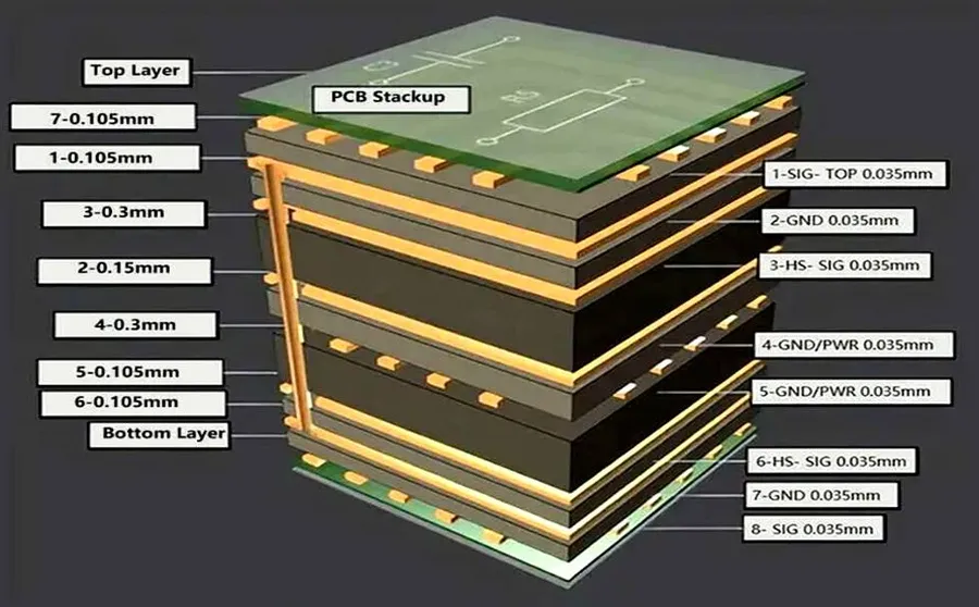
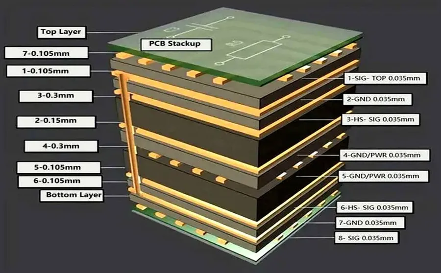
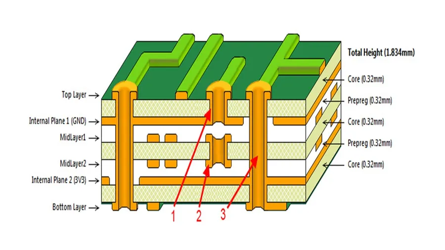
A multilayer PCB (Printed Circuit Board) is a circuit board composed of three or more conductive layers, each separated by an insulating layer. This layered structure allows for increased circuit density and complexity compared to single or double-layer PCBs, facilitating the design of compact and high-performance electronic devices. The minimum number of layers is typically three, but PCBs with 50 or more layers are not uncommon in advanced applications.
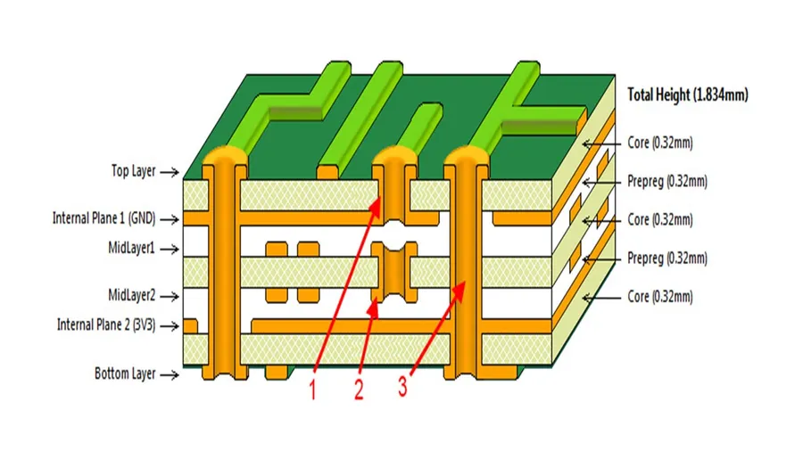
The conductive layers, usually made of copper, are patterned with circuits using etching processes. These layers are then laminated together with prepreg, a bonding material consisting of resin-impregnated fiberglass. Core materials like FR-4 provide structural support to the PCB. The choice of these materials is critical to PCB performance and intended application.
How Multilayer PCBs Are Manufactured
PCB Manufacturing Process
The fabrication of multilayer PCBs is a complex process involving several stages of precision manufacturing. These steps ensure the creation of intricate circuits necessary for modern electronics, encompassing layer stacking, lamination, drilling, plating, and etching, each executed with specific materials and techniques.
Below is a detailed breakdown of the key manufacturing stages:
1. Layer Stacking The process begins with the preparation of individual layers, typically made of copper-clad laminates. These layers are patterned with the circuit design through a photo-imaging process. This involves applying a photosensitive resist, exposing it to UV light through a photomask, and then removing the unexposed resist to reveal the copper areas that will form the circuits.
2. Lamination Once the inner layers are patterned, they are stacked together with prepreg (a partially cured fiberglass epoxy) as a bonding material. This stack-up is subjected to high temperature and pressure in a lamination press, causing the prepreg to melt and bond the layers together. The precise alignment and uniform pressure are critical in avoiding any air gaps or delaminations within the finished product. The layer stack up is dependent on many factors and can be complex with varying copper thicknesses and dielectric materials and thicknesses.
3. Drilling Following lamination, vias and through-holes are created using precision drilling equipment. These holes establish electrical connections between different layers. High-speed drills with carbide or diamond-coated bits are employed, and accurate positioning is vital to avoid damage to the circuits. The diameter and position of each hole is critical to maintaining the quality of the final product. After the drilling process the walls of the holes are rough, making it difficult to plate. A chemical or mechanical process called 'desmearing' is used to remove any residual resin and roughen the hole walls in preparation for the plating stage.
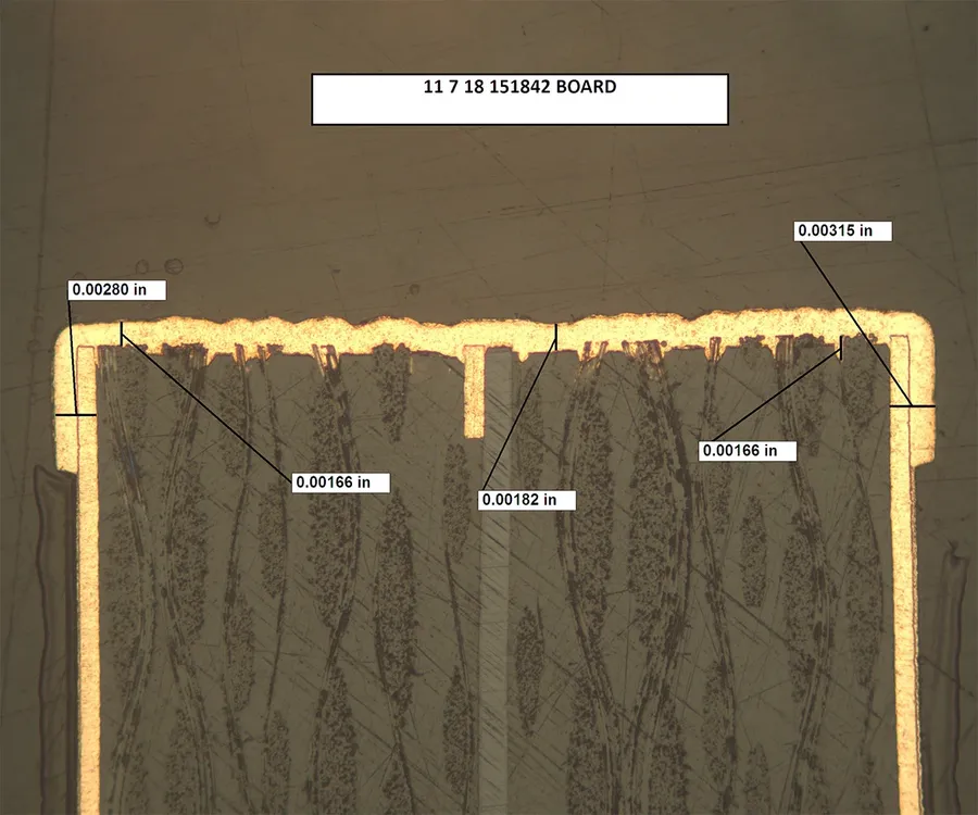
4. Plating The drilled holes are made conductive through an electroplating process, where copper is deposited on the hole walls and surface. This creates an electrical pathway from one layer to the next, connecting the copper traces from layer to layer. The plating process requires careful monitoring of current density and chemical concentrations to ensure a consistent and reliable copper deposit. This plated copper creates the needed electrical pathway from layer to layer.
5. Etching After plating, the outer layers are processed. A thin film of photosensitive resist is applied, imaged, and the resist is developed to reveal the areas of copper to be removed. The revealed copper is then etched away, using a chemical etchant, leaving behind the final circuit traces and pads. After etching the resist is removed and the printed circuit board is ready for the next stage of manufacturing.
6. Solder Mask Application and Surface Finishing A solder mask is applied to the surface of the PCB to protect the circuit traces from oxidation and to prevent solder from bridging between pads during component assembly. Then, a surface finish such as HASL, ENIG, or immersion tin is applied to the exposed copper to improve solderability and corrosion resistance.
Advantages of Multilayer PCBs
Multilayer PCB Cross Section
Multilayer PCBs offer significant advantages over single- and double-layer boards, primarily due to their increased layer count which enables higher circuit density and improved performance. These benefits stem from the ability to create complex routing patterns within the multiple layers of the board, which is vital for sophisticated electronic applications.
Advantage
Description
Impact
Increased Density
Multiple layers allow for a greater number of components and interconnections in a given area.
Enables smaller, more compact devices with complex functionality.
Reduced Size and Weight
By integrating more functionality into fewer layers, the overall PCB size and weight can be reduced.
Crucial for portable devices and applications with space constraints.
Improved Electrical Performance
The multi-layered structure allows for better control of impedance and signal integrity, reducing signal loss and cross-talk.
Ensures reliable and high-speed data transfer, suitable for demanding applications.
Enhanced Signal Integrity
Dedicated ground and power planes within the multilayer structure minimize noise and interference, resulting in cleaner signals.
Critical for high-frequency circuits and sensitive applications.
Increased Design Flexibility
More layers provide greater flexibility for signal routing and component placement.
Allows for more complex designs with increased functionality
Applications of Multilayer PCBs
Devices using multilayer PCBs
Multilayer PCBs, owing to their compact size, high density, and excellent electrical performance, find extensive use across a diverse range of industries. These advanced circuit boards are integral to applications requiring complex circuitry within confined spaces.
Below we outline some key application areas.
Consumer Electronics Multilayer PCBs are essential in smartphones, tablets, laptops, and other portable devices, where size and weight are critical factors. They facilitate the integration of various components, such as processors, memory, and communication modules, into a compact form factor.
Aerospace and Defense In aerospace and defense, multilayer PCBs are utilized in avionics, radar systems, and satellite communication equipment. The demand here is for high reliability and performance, often under extreme environmental conditions. Their compact form-factor and robustness makes them ideal for such conditions.
Automotive Industry Modern automotive systems, including engine control units (ECUs), infotainment systems, and advanced driver-assistance systems (ADAS), heavily rely on multilayer PCBs. These PCBs must endure harsh operating conditions, including temperature variations and mechanical stress while maintaining high performance and reliability.
Medical Devices Multilayer PCBs are crucial components in medical imaging equipment, diagnostic tools, and implantable devices. These applications require high precision, reliability, and often adhere to stringent regulatory standards for safety and performance.
Telecommunications Networking equipment, routers, and base stations depend on multilayer PCBs to handle high-speed data transmission. These PCBs must provide excellent signal integrity and noise immunity to meet the demands of high-bandwidth communication.
Industrial Automation In industrial settings, multilayer PCBs are used in control systems, robotics, and manufacturing equipment. These environments often require robust PCBs that can withstand harsh conditions and ensure reliable operation.
High Performance Computing Multilayer PCBs are fundamental to high-performance computing, used in data centers, servers, and workstations. They facilitate the dense integration of processors, memory, and communication interfaces for optimal performance.
Design Considerations for Multilayer PCBs
PCB Layout Design
Effective multilayer PCB design is crucial for achieving optimal performance, encompassing meticulous planning of layer stack-up, controlled impedance, efficient signal routing, diligent thermal management, and strategic component placement to ensure the circuit board functions as intended.
Design Parameter
Description
Importance
Layer Stack-up
Arrangement and order of conductive and insulating layers
Impacts impedance, signal integrity, and manufacturing feasibility. Balanced stack-ups minimize warpage.
Impedance Control
Maintaining a consistent characteristic impedance for signal traces
Prevents signal reflections, ensuring clean signal transmission and reducing signal loss. Critical for high-speed signals.
Signal Routing
Planning the path of electrical signals across the layers
Reduces interference and crosstalk, optimizes signal paths for minimized delay and reduced signal loss.
Thermal Management
Strategically dissipating heat generated by components
Prevents overheating, ensures component reliability, prolongs lifespan, and maintains performance. Thermal vias and heat sinks are commonly used.
Component Placement
Strategic positioning of components on the board
Optimizes performance and functionality, reduces signal path lengths, enables efficient manufacturing, and enhances accessibility.
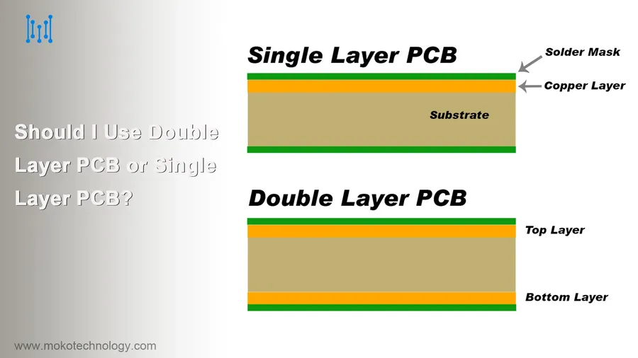
Multilayer PCB vs. Single and Double Layer PCBs
PCB Layer Comparison
Multilayer PCBs, single-layer PCBs, and double-layer PCBs represent distinct tiers of circuit board complexity, each suited to different applications based on performance, density, and cost requirements. This section provides a comparative analysis to clarify the trade-offs between these technologies.
This section addresses common queries regarding multilayer PCBs, providing concise and technically accurate answers to enhance understanding and assist in decision-making processes related to their application.
What are the main disadvantages of using multilayer PCBs? While offering significant advantages, multilayer PCBs also present certain drawbacks. Key disadvantages include increased manufacturing cost and complexity, extended lead times, and potentially higher susceptibility to manufacturing defects due to their intricate layered structure. Additionally, rework and repair can be considerably more challenging compared to single or double-layer PCBs.
What are the fundamental differences between single-layer and multilayer PCBs? The core distinction lies in their construction. Single-layer PCBs feature a conductive layer on one side of the substrate, whereas multilayer PCBs consist of three or more conductive layers separated by insulating material. This difference in structure leads to significant variations in density, functionality, signal integrity, and application suitability. Multilayer boards allow for higher circuit density and complexity within a given area.
Where are multilayer PCBs commonly utilized? Multilayer PCBs find extensive use in applications requiring high circuit density and performance. They are prevalent in industries such as aerospace, where miniaturization and reliability are critical; in advanced consumer electronics (smartphones, tablets); in high-speed computing and networking equipment; and in sophisticated medical devices where precision and compact design are essential.
How does the cost of a multilayer PCB compare to a single-layer or double-layer PCB? Multilayer PCBs typically cost more than single-layer or double-layer boards due to the increased manufacturing complexity, additional materials, and precision processes involved in their fabrication. The cost increase is usually directly proportional to the number of layers and the complexity of the design.
What design considerations are particularly crucial for multilayer PCBs? Designers must pay close attention to layer stack-up to manage impedance and signal integrity. Proper thermal management is essential to dissipate heat. Routing and trace impedance should be carefully planned to avoid signal interference, and component placement should optimize performance and manufacturability. Controlled impedance is also important in high frequency circuits.
Can multilayer PCBs be used for high-frequency applications? Yes, multilayer PCBs are well-suited for high-frequency applications due to their ability to provide controlled impedance and minimize signal reflections through careful layer stack-up and design. The increased number of layers allows for better power and ground plane design, which is beneficial for maintaining signal integrity in high-speed circuits.
Are there any limitations in the number of layers that can be incorporated into a multilayer PCB? While technology is advancing rapidly, there are practical limitations to the number of layers in a multilayer PCB. Very high layer counts can increase cost, reduce yield and present significant assembly challenges. The actual limit depends on the manufacturing technology, materials used, and intended application.
Cost Factors in Multilayer PCB Manufacturing
The cost of manufacturing multilayer PCBs is influenced by several interconnected factors, extending beyond simple material expenses to encompass design complexity and production scale. Understanding these elements is crucial for effective project budgeting and cost optimization.
Cost Factor
Description
Impact on Cost
Layer Count
The total number of conductive layers in the PCB.
Directly proportional to cost. More layers require more material, processing steps, and complexity.
Material Type
The specific dielectric and conductive materials used.
Advanced materials like high-Tg FR-4 or specialized laminates increase cost compared to standard materials.
PCB Size and Thickness
The physical dimensions and overall thickness of the PCB.
Larger PCBs consume more material and require more processing time, leading to higher costs. Thicker boards also impact material consumption and processing.
Manufacturing Complexity
The intricacy of design features, such as microvias, blind/buried vias, fine lines, and controlled impedance requirements.
Complex designs require more precise manufacturing and advanced equipment which results in higher costs.
Surface Finish
The type of plating or finish applied to the surface of the PCB (e.g., ENIG, HASL, immersion silver).
Some finishes, like ENIG, are more costly due to the materials and processes used.
Drilling Complexity
The number and size of drilled holes, including microvias and blind/buried vias.
Higher hole counts, smaller hole sizes, and non-standard vias increase the cost due to the precision required.
Production Volume
The number of PCBs being produced in a single run.
Larger production volumes typically lead to lower per-unit costs due to economies of scale.
Lead Time
The turnaround time for PCB manufacturing.
Faster lead times or expedited manufacturing processes increase costs due to the prioritization of production.
Testing Requirements
The testing needed for the PCB, including electrical testing and functional testing.
More rigorous testing protocols and specialized testing equipment increase the costs.
Future Trends in Multilayer PCB Technology
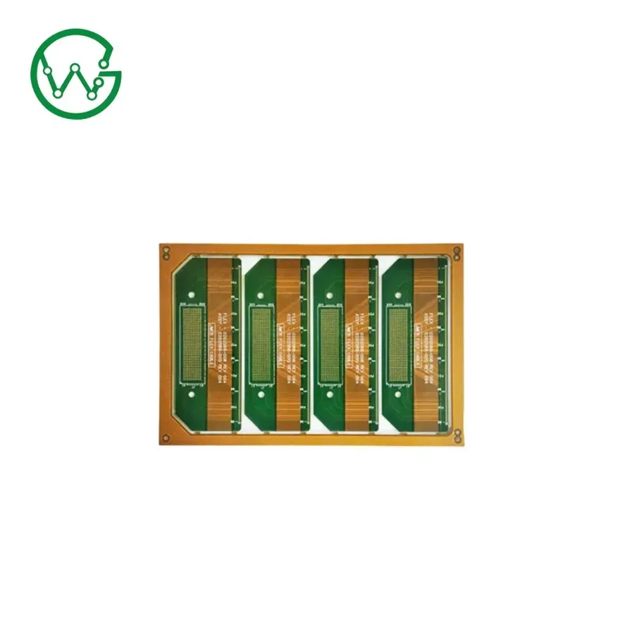
Flexible Multilayer PCB
The multilayer PCB industry is continually evolving, driven by the ever-increasing demands for higher performance, miniaturization, and enhanced functionality in electronic devices. Key trends are pushing the boundaries of what's achievable in circuit board design and manufacturing, incorporating advanced materials, fabrication methods, and interconnect strategies.
High-Density Interconnect (HDI) HDI technology is at the forefront, enabling finer lines, smaller vias, and increased component density. This leads to smaller PCBs with more complex circuitry, crucial for applications like smartphones, wearables, and portable medical devices. Advanced microvia technology and laser drilling methods are vital components of HDI advancements.
Flexible and Rigid-Flex PCBs Flexible PCBs and rigid-flex designs are rapidly gaining traction. Their ability to conform to complex shapes and fit within confined spaces opens new possibilities for product design. These flexible substrates utilize materials such as polyimide or polyester films. They are essential in automotive, aerospace, and wearable technologies where space and weight are critical factors.
Advanced Materials Research into advanced materials is critical for improving signal integrity, thermal management, and durability. Materials with lower dielectric constants and loss tangents are being adopted for high-speed applications. The use of thermally conductive substrates and fillers improves heat dissipation, extending the operational life of the PCB. Examples include advanced ceramics, filled epoxy resins, and modified PTFE laminates.
Embedded Components Embedding passive and active components within the PCB layers further enhances miniaturization and reduces parasitic effects. This approach integrates components directly within the PCB layers, reducing the overall size and improving electrical performance. Techniques involve careful control over via formation, surface finishing, and precise component assembly.
3D Printing of PCBs Additive manufacturing, or 3D printing, is emerging as a potential method for rapid prototyping and creating complex PCB geometries. Although still in the early stages, this method offers the potential to rapidly manufacture custom PCBs with unique shapes and designs. Direct ink writing, material extrusion, and vat photopolymerization are some of the 3D printing techniques being explored.
Multilayer PCBs have revolutionized modern electronics by enabling intricate circuits in compact spaces. Understanding their design, manufacturing, and applications is crucial for engineers and enthusiasts alike. As technology evolves, the role of multilayer PCBs will only continue to expand, driving innovation across various industries and pushing the boundaries of what is possible in electronics. The benefits of multilayer PCBs outweigh many other technologies and will continue to be a key component of our future.