In today's fast-paced world of electronics, the ability to quickly prototype and create custom PCBs is invaluable. Laser engraving PCBs offers a precise and accessible method, bridging the gap between design and reality. This article dives deep into the techniques, challenges, and solutions for effectively using laser engravers in PCB fabrication, combining the allure of laser technology with the practicality of circuit board development to unveil its potential for hobbyists and professionals alike.
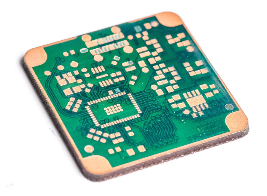
Laser engraving for Printed Circuit Boards (PCBs) leverages the precision of focused laser beams to selectively remove material, typically a resist layer, revealing the underlying conductive copper for subsequent etching. This method offers a rapid and highly accurate alternative to traditional subtractive PCB fabrication techniques, allowing for intricate designs and rapid prototyping.
The fundamental principle involves using a laser to ablate a thin layer of material, where the laser's energy is converted into heat, causing the material to vaporize or decompose. This precise material removal enables the creation of the desired circuit patterns on the PCB. The effectiveness of laser engraving is dependent on several factors, including the type of laser, its power, wavelength, and the material properties of both the resist layer and the PCB substrate.
| Aspect | CO2 Laser | Fiber Laser |
|---|---|---|
| Wavelength | 10.6 μm (Infrared) | 1.064 μm (Near-Infrared) |
| Material Suitability | Effective for organics like resist materials. Less ideal for metals | Ideal for metals (like copper), can be used with some resist materials |
| Beam Diameter | Typically larger, resulting in broader cut widths | Typically smaller, enabling finer features and more precise cuts |
| Power | Lower power needed for organic resist ablation | Higher power generally required, better for metals |
| Cost | Generally lower initial cost | Generally higher initial cost |
| Complexity | Simpler design and maintenance | More complex setup and maintenance |
| Applications in PCB | Primarily for resist ablation, less effective for direct metal removal | Directly engraving copper, precise microvia creation and metal removal |
Compared to traditional PCB fabrication methods such as chemical etching, laser engraving provides several advantages. It enables rapid prototyping and design iterations, allows for precise control over feature dimensions, and reduces the need for harmful chemicals. However, it also presents certain limitations, including higher initial investment costs for equipment, potential challenges with very fine feature sizes depending on the laser type and material, and the need for careful parameter calibration.
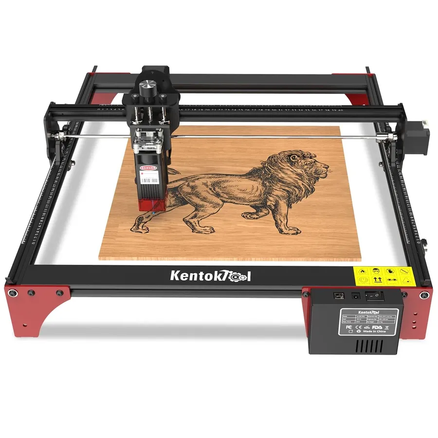
Selecting the appropriate laser engraver for PCB fabrication is crucial for achieving precise and cost-effective results. This section provides a detailed comparison of CO2 and fiber lasers, focusing on their suitability for PCB etching, while considering factors such as power, wavelength, and overall cost-effectiveness to guide you in making an informed decision based on your budget and specific project needs.
| Feature | CO2 Laser | Fiber Laser |
|---|---|---|
| Wavelength | 10.6 μm (Infrared) | 1.06 μm (Near-Infrared) |
| Material Compatibility | Suitable for organic materials, less effective on metals | Highly effective for metals and some plastics |
| PCB Etching Suitability | Can etch resist materials, but less efficient on copper | Excellent for direct copper etching if powerful enough, otherwise good for resist |
| Power Output | Typically available in a range of power levels suitable for resist removal | Available in a range of power, suitable for resist removal and some direct copper etching |
| Precision | Good for resist removal, but may require multiple passes for precise copper etching. | Higher precision, better for intricate patterns |
| Cost | Generally lower upfront cost, but ongoing maintenance can be higher. | Higher upfront cost, but lower maintenance over time and higher productivity |
| Maintenance | Requires periodic gas refills and optical alignment. | Generally lower maintenance and longer lifespan |
When considering cost, note that while CO2 lasers often have a lower initial investment, the operational costs can be higher due to the need for gas refills and more frequent maintenance. Fiber lasers, while pricier upfront, often offer better efficiency, lower maintenance, and longer lifespan, potentially resulting in lower long-term costs, particularly when directly etching copper, although very few can reach this power level without extremely high cost, resist is the more common option.
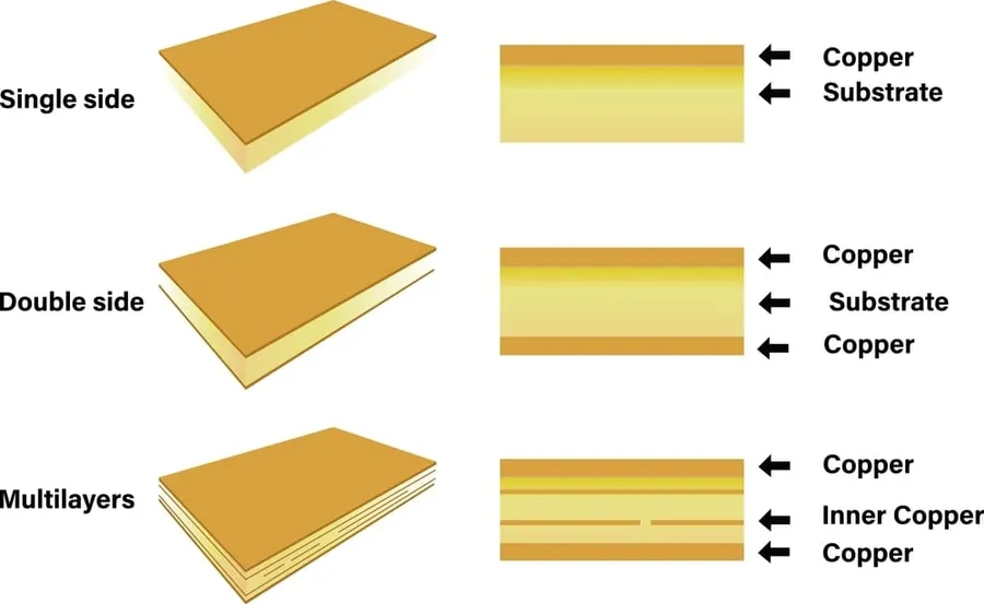
Successful laser engraving of PCBs hinges critically on the selection of appropriate materials and meticulous preparation. This section details the essential materials—copper clad laminates and resist materials—and outlines the necessary preparation steps, including resist application, cleaning, and surface treatments, to ensure optimal laser etching outcomes.
| Material | Description | Laser Compatibility |
|---|---|---|
| Copper Clad Laminates (CCL) | Base substrate for PCBs, typically FR-4 (fiberglass reinforced epoxy) with copper layers on one or both sides. | Compatible with both CO2 and Fiber lasers; Fiber lasers may offer greater precision for fine detail. |
| Photoresist | Light-sensitive coating used to create a protective layer for etching; available in various types (e.g., dry film, liquid) | Absorbs laser energy effectively for ablation; optimal thickness and composition vary by specific laser and application. |
| Laserable spray paint | An alternative to photoresist, applied evenly for laser etching. Must be laser-compatible to avoid residue or fumes. | Compatible with CO2 lasers; some formulations may be suitable for Fiber lasers at controlled power levels. |
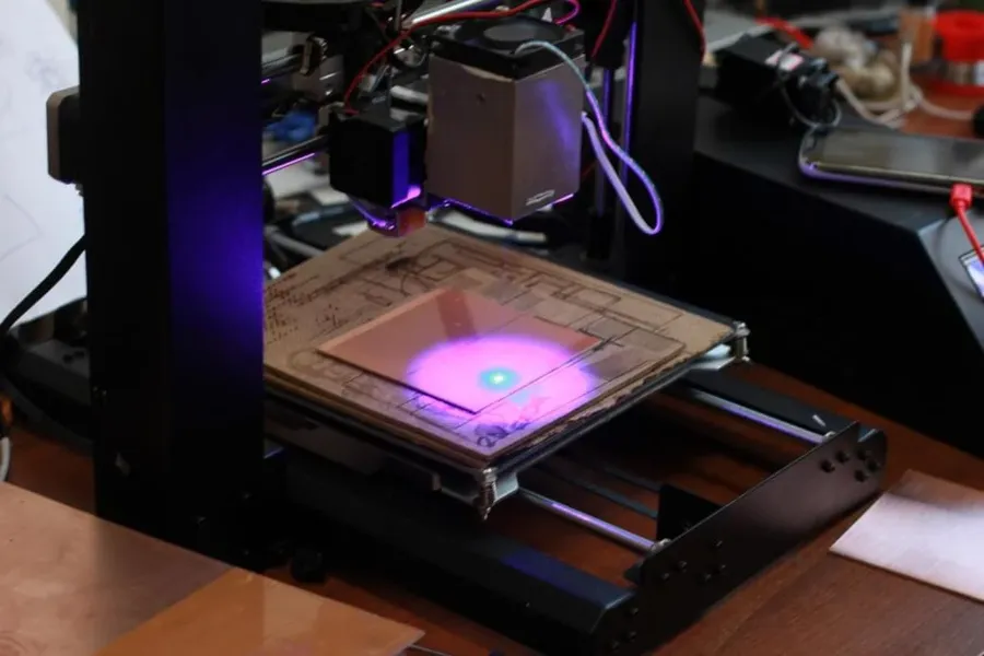
Laser PCB engraving is a precise process requiring careful execution from design to final product. This section provides a structured, step-by-step guide to ensure successful laser engraving of printed circuit boards, covering critical aspects such as file preparation, laser parameter settings, and post-engraving procedures.
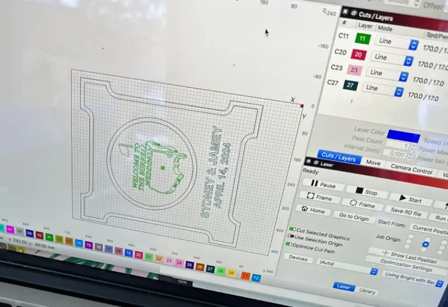
The precision of laser engraving for PCB fabrication hinges not only on the hardware but critically on the software and file preparation process. This stage is pivotal for translating CAD designs into accurate laser paths, optimizing for laser engraving parameters, and ensuring the successful transfer of design intent to the physical board.
The workflow typically involves exporting designs from CAD software like KiCad or Eagle into formats compatible with laser engraving software. This often requires converting complex PCB layouts into simplified vector graphics, adjusting for line thicknesses, clearances, and other design parameters specific to laser etching, and ensuring compatibility with the specific laser machine.
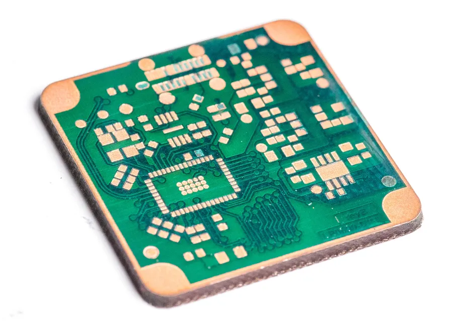
Achieving precision in laser PCB engraving requires careful attention to several factors that can lead to common issues such as over-etching, under-etching, and alignment inaccuracies. These challenges are often overcome through meticulous calibration, material testing, and the implementation of strategic techniques to ensure consistent, high-quality results. By understanding and addressing these issues, one can optimize the laser engraving process for effective and reliable PCB fabrication, while adhering to critical safety measures to mitigate potential hazards.
| Challenge | Description | Potential Causes | Solutions |
|---|---|---|---|
| Over-etching | Excessive material removal, resulting in widened traces and potential short circuits. | Excessive laser power, slow scanning speed, multiple passes, incorrect material settings. | Reduce laser power, increase scanning speed, optimize number of passes, calibrate material settings. |
| Under-etching | Insufficient material removal, leading to incomplete trace separation and potential connectivity issues. | Insufficient laser power, high scanning speed, incorrect material settings, inadequate resist. | Increase laser power, reduce scanning speed, optimize material settings, verify resist application. |
| Alignment problems | Misalignment between design file and the physical PCB, leading to errors in trace placement. | Inaccurate setup, improper fixturing, errors in software calibration, material movement during process. | Ensure accurate alignment, use precision fixturing, correct software calibration, stabilize material during process. |
| Inconsistent Etching | Variations in etching depth or width across the PCB. | Uneven laser beam intensity, variations in material properties, unstable laser performance, inconsistent resist application. | Calibrate beam intensity, ensure material uniformity, verify laser stability, improve resist application process. |
| Residue or charring | Burned material left on the PCB surface after etching. | Excessive laser power, slow scanning speed, improper material settings, inadequate air assist. | Reduce laser power, increase scanning speed, optimize material settings, enhance air assist to remove debris. |
Safety precautions are paramount when operating laser engraving equipment. Always wear appropriate laser safety glasses to protect your eyes from harmful radiation. Ensure proper ventilation to remove any fumes produced during the process and avoid contact with the laser beam, as it can cause serious burns and irreversible damage. Familiarize yourself with the specific safety guidelines of your laser equipment and adhere to them strictly.
This section addresses common queries regarding laser engraving of PCBs, providing clear and concise answers to help users understand the process, its limitations, and best practices.
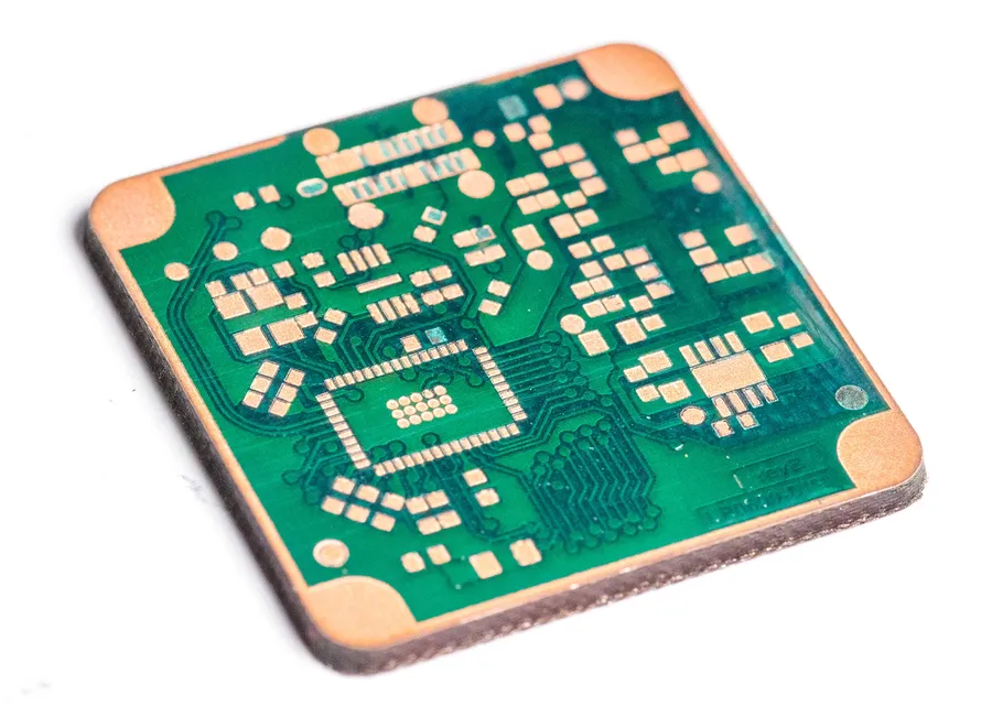
Laser engraving is not limited to single-layer PCBs; its precision enables the creation of multi-layer boards and intricate patterns, pushing the boundaries of PCB fabrication. This section delves into these advanced applications and the synergy between laser engraving and traditional manufacturing methods.
Multi-layer PCB fabrication with laser engraving involves selectively removing resist from multiple layers of copper clad laminate. This requires precise alignment between layers, often achieved with fiducial markers. The process allows for the creation of vias, interconnections between layers, and intricate signal traces, demonstrating the versatility of laser engraving in complex circuit designs.
Beyond multi-layer boards, laser engraving excels in creating specialized features, such as microfluidic channels, fine pitch component pads, or unique shapes on the PCB. The ability to control the laser's path and power with precision makes it suitable for customized solutions that traditional etching methods struggle to achieve.
The combination of laser engraving and traditional PCB manufacturing techniques offers numerous advantages. For example, laser engraving can be used for prototyping or fine-tuning specific areas, with mass production handled by conventional processes. This hybrid approach leverages the benefits of both techniques: precision and flexibility from laser engraving, and scalability and cost-effectiveness from conventional manufacturing methods.
Laser direct structuring (LDS) is a notable technique where laser engraving creates a pattern on a plastic part, which is then metallized. This method can create 3D circuits, integrating electronics directly into the structural components of a device. While not directly PCB fabrication, LDS shares the core laser engraving principles and showcases the expanded potential of this technology.
| Feature | Laser Engraving | Traditional Etching |
|---|---|---|
| Multi-Layer Capability | High precision for complex multi-layer | Standard process, limited precision |
| Intricate Patterns | Excellent for fine lines and unique designs | Challenging for very fine or non-standard shapes |
| Prototyping Flexibility | Ideal for quick design changes and adjustments | More time-consuming for revisions |
| Hybrid Manufacturing | Seamlessly integrates with traditional methods for optimal results | Requires separate processing for fine details |
The landscape of laser-engraved PCBs is poised for significant evolution, driven by advancements in materials science, laser technology, and process optimization. These innovations promise to enhance precision, efficiency, and the scope of applications for laser-based PCB fabrication.
Emerging trends are focusing on several key areas:
These advancements promise to address many limitations of current laser engraving technology, offering greater precision and higher efficiencies, thus, paving the way for future development of PCB manufacturing techniques. As a result, laser engraving will become an increasingly important part of PCB production.
Laser engraving PCBs offers a powerful blend of precision and accessibility, empowering makers with the means to rapidly prototype and fabricate circuits. From understanding the core principles to mastering advanced techniques, the ability to laser engrave PCBs provides a versatile skill set for those seeking to push the boundaries of circuit board creation. As laser technology advances, this method will become even more instrumental in shaping the future of electronics manufacturing. By embracing both innovation and precision, you can fully realize the potential of laser engraving in your PCB design and production journey.

