In the realm of electronics, the journey from concept to a finished product often begins with a proto pcb. Like an architect's blueprint for a building, proto PCBs allow engineers and hobbyists to test their designs before committing to mass production. This article will guide you through the ins and outs of proto PCBs, explore their significance, and offer advice on how to approach your first prototyping projects. Just like how the first sketches of a new invention mark its debut, proto PCBs are the crucial first step to verifying your electronic circuits.
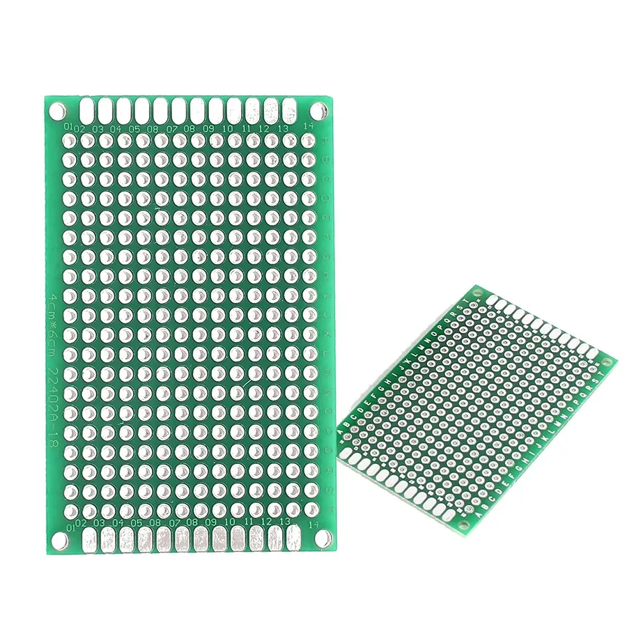
A proto PCB, or prototype printed circuit board, is a pre-production version of a circuit board used to validate designs, test functionality, and refine layouts before committing to full-scale production. It serves as a crucial intermediate step, bridging the gap between theoretical designs and mass-produced electronics, offering a tangible platform for experimentation and iterative improvement.
The significance of proto PCBs lies in their ability to mitigate risks and costs associated with mass production. By thoroughly testing a prototype, engineers can identify and correct design flaws, component incompatibilities, or performance issues early in the development cycle. This proactive approach significantly reduces the likelihood of costly recalls, redesigns, and production delays further down the line, ultimately saving time and resources.
| Feature | Proto PCB | Production PCB | Breadboard |
|---|---|---|---|
| Purpose | Design validation and testing | Mass production | Initial circuit exploration |
| Durability | Moderate | High | Low |
| Component Mounting | Solderable, permanent | Solderable, permanent | Plug-in, temporary |
| Layout Flexibility | Limited to design | Fixed layout | Highly flexible |
| Cost | Low to moderate | Moderate to High | Low |
| Complexity | Designed for specific circuit | Complex designs | Simple circuits |
| Application | Before mass production | For final products | Proof of concept |
Proto PCBs differ significantly from both production PCBs and breadboards. Unlike breadboards, which are temporary and unsuitable for permanent circuit implementations, proto PCBs offer a solderable and more robust platform. While production PCBs are intended for final, mass-produced products, proto PCBs are created for iterative design and testing. Proto PCBs are specifically for validating the design and functionality before the production stage.
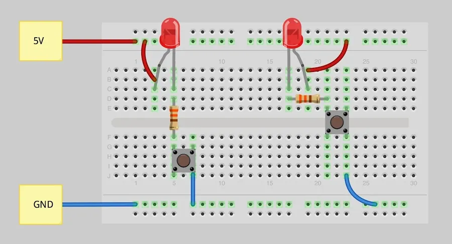
Proto PCBs serve as a crucial intermediary step between theoretical circuit design and mass production, offering a physical platform to test and validate electronic circuits. Various types cater to different prototyping needs, from simple educational projects to complex industrial applications. These types can be broadly categorized into perma-proto boards, breadboard-style PCBs, and custom-designed PCBs, each with unique advantages and disadvantages.
| Type of Proto PCB | Description | Pros | Cons | Typical Applications |
|---|---|---|---|---|
| Perma-Proto Boards | Also known as perfboards, these have a grid of plated-through holes, often with power rails, allowing for solder connections. | Versatile for various projects, good for permanent prototypes, allows for more complex circuits than breadboards. | Can be time-consuming to solder, less flexible than breadboards for quick changes, require soldering skill. | Educational projects, simple circuits, permanent prototypes of moderate complexity. |
| Breadboard-Style PCBs | Feature conductive tracks and spring-loaded sockets similar to a standard breadboard, enabling solderless connections. | Extremely flexible for rapid prototyping, easy to change circuits quickly, no soldering is required. | Can be limited in terms of component types and complexity, connections can be unreliable in the long term, can be bulky. | Quick and easy tests, temporary and rapid prototyping, initial circuit validation. |
| Custom-Designed PCBs | These are PCBs designed to your specific requirements, usually fabricated using a PCB design software. | Highly tailored for specific application, allows for advanced circuit designs (multi-layer), can be optimized for performance. | Longer turnaround time, requires proficiency in PCB design software, higher initial cost. | Complex circuits, finalized prototype development, projects with specific performance requirements, high density electronics. |
Selecting the right proto PCB manufacturer is critical for ensuring that your design moves smoothly from concept to functional prototype. This choice impacts not only the quality of your boards but also the overall project timeline and budget. Careful consideration of factors like cost, turnaround time, technical capabilities, and quality is essential to avoid costly delays and ensure reliable prototype performance.
| Factor | Description | Impact |
|---|---|---|
| Cost | The total expense for manufacturing, including setup fees, per-board costs, and any additional services. | Directly affects the project budget; cheaper options may compromise quality and vice-versa. |
| Turnaround Time | The duration from when you place your order to when you receive the finished boards. | Impacts the project timeline and speed of iteration cycles; longer times can cause critical project delays. |
| Board Complexity | The number of layers, board size, and other design specifications such as the smallest track and gap size. | Determines if the manufacturer can produce your design; some manufacturers have limits on board layer count and design feature sizes. |
| Material Quality | The type of material used (e.g., FR-4, Rogers) and its quality standards. | Affects board performance, durability, and reliability; higher-quality materials typically offer better performance but are more costly. |
| Manufacturer Capability | The manufacturing technologies and process offered (e.g., SMT assembly, plated holes). | Determines what services are available; specialized needs may require a more advanced manufacturer. |
| Quality Standards | Certifications (e.g., ISO 9001) and quality control practices of the manufacturer. | Ensures consistency and reliability of the PCB; higher standards translate to fewer defective boards. |
| Online Platform | The usability, features, and customer service provided by online platforms of various manufacturers. | Impacts the ease of ordering, communication, and tracking the manufacturing process; user-friendly online platforms can save time and effort. |
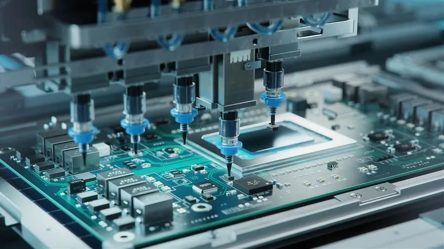
Creating a proto PCB involves a structured process encompassing design, fabrication, and assembly. This iterative process is crucial for validating electronic designs before mass production. It ensures that the final product meets performance and functional requirements, minimizing costly revisions down the line.
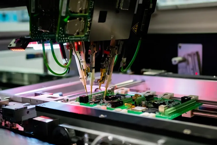
Effective proto PCB design for testing and iteration is crucial for streamlining the development process. By incorporating design for testability (DFT) principles and strategic planning, designers can significantly reduce debugging time and facilitate multiple design revisions. This approach ensures that prototypes can be easily tested, analyzed, and improved.
This section addresses common inquiries regarding prototype PCBs (Proto PCBs), offering clear and concise answers to help you navigate the world of circuit board prototyping. These questions range from basic definitions to practical considerations, ensuring a comprehensive understanding of proto PCBs.
Optimizing costs in proto PCB fabrication is crucial for both hobbyists and businesses. While quality is paramount, several strategies can be employed to reduce expenses without compromising the functionality of the prototype. This section will delve into these strategies, including pricing structures, panelization, standard board sizes, and the impact of order quantity.
| Cost Factor | Description | Cost Reduction Strategy |
|---|---|---|
| Board Size | The physical dimensions of the PCB significantly impact the material used and processing time. | Utilize standard sizes or panelize multiple small PCBs into a larger standard sized panel. |
| Number of Layers | Layer count directly correlates with complexity and processing cost. | Start with the fewest layers required to meet circuit design needs, and add more only when necessary. Use 2-layer boards when possible |
| Material | Different materials have different costs and will affect the thermal/electrical performance of the PCB. | Choose cost-effective but standard materials like FR4 for general prototyping, especially when high thermal or electrical performance is not required. |
| Lead Time | Standard or longer lead times usually mean lower costs. | Avoid expedited shipping unless time is absolutely critical; standard lead time will result in lower cost per PCB. |
| Surface Finish | Different surface finishes (e.g. ENIG, HASL) can significantly affect the cost. | Use less expensive HASL finish when appropriate, ENIG finish is used for high reliability applications. |
| Panelization | Panelization combines multiple PCBs into a single large board, thus reducing manufacturing costs. | When ordering many copies of a design, design as a panel for automated assembly and lower fabrication costs. |
| Quantity | The quantity of PCBs ordered influences the unit price. Higher quantity, typically lower unit price. | Order multiple copies of a design as soon as the design is proven, to take advantage of quantity discounts. |
Understanding different pricing structures from proto PCB manufacturers is essential. Some manufacturers charge based on board area, while others may have fixed fees with added costs for extras such as vias, slots, and cutouts. Comparing quotes from various manufacturers using the above table will be an important part of your cost reduction strategy.
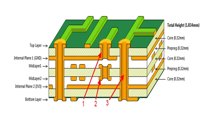
While through-hole components are often used in initial prototyping, advanced proto PCB techniques, such as surface mount technology (SMT) assembly and multi-layer PCB design, offer significant advantages for more complex and compact prototypes. These techniques, while more involved, enable a closer representation of a final product's performance and size, and they can also refine a product's ability to manage heat and maintain signal integrity even at a basic prototype level.
Surface Mount Technology (SMT) involves soldering components directly onto the surface of the PCB. This method provides higher component density, allowing for smaller board sizes and potentially lower assembly costs in larger quantities. While SMT assembly for prototype PCBs can present challenges, the benefits of a more compact design often outweigh these difficulties.
Multi-layer PCBs involve stacking multiple layers of conductive material (typically copper) separated by insulating layers. This allows for greater routing flexibility, enabling complex designs to be achieved on smaller PCBs. Multi-layer prototypes are essential for high-speed digital circuits, RF designs, or any application that requires substantial routing density, controlled impedance, and can also enhance power distribution.
| Feature | SMT Assembly | Multi-Layer PCBs |
|---|---|---|
| Component Density | High, allows for smaller PCBs | Higher trace density, smaller PCBs with more functionality |
| Assembly Complexity | Requires specialized equipment, but more cost effective at higher quantities | More complex fabrication |
| Routing Flexibility | Limited to surface traces on a single side | Enhanced with multiple layers, enabling complex routing patterns |
| Best Use Cases | Compact designs, mass production | Complex designs, high-speed signals, and noise sensitive applications. |
| Thermal management | Components are on surface, potentially less efficient heat dissipation than multi-layer | Additional layers can be strategically used to enhance thermal dissipation. |
| Signal Integrity | Potentially more susceptible to noise and signal degradation at high frequencies | Allows for impedance control and better signal routing for better signal quality |
Both SMT assembly and multi-layer PCB design introduce design considerations like thermal management and signal integrity. With SMT, using vias under thermal pads can help dissipate heat from the component. For multi-layer designs, ensuring signal integrity means careful layer stacking, trace impedance control, and appropriate use of ground planes. Although this applies to final product, consideration of this even in the proto phase will allow for easier transition into final product.
The field of proto PCB technology is rapidly evolving, driven by advancements in materials, fabrication techniques, and automation. These trends are poised to significantly impact how prototypes are developed and iterated, enabling faster, more efficient, and more complex designs. These changes will enhance both the capabilities and accessibility of PCB prototyping.
The proto pcb stands as the cornerstone of innovation in electronics. Understanding its importance, various types, and manufacturing process is vital for any hardware developer. By optimizing your design, choosing the right fabrication process, and keeping up with technological advancements, you can ensure that your journey from idea to product is smooth and successful. This is the foundation for turning electronic dreams into reality, whether you are using simple proto boards or more advanced proto pcbs. Embrace the proto pcb, your first step toward bringing your innovative circuit designs to life.

