The backbone of modern electronics, printed circuit boards (PCBs) are essential for connecting electronic components. From smartphones to complex industrial machinery, PCBs enable the functionality we rely on daily. This guide will take you through the entire PCB making journey, exploring design principles, manufacturing processes, and practical tips for creating your own circuits, demystifying the process for both hobbyists and professionals alike.
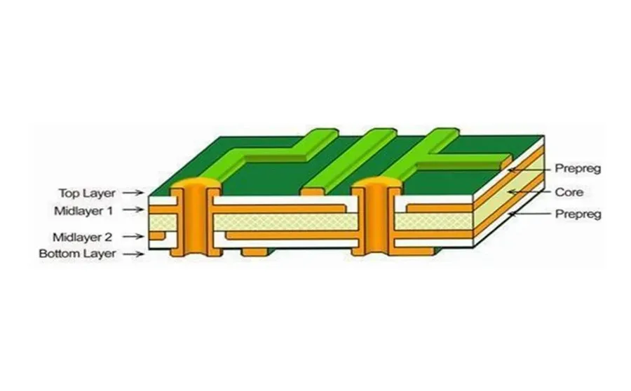
Printed Circuit Boards (PCBs) form the backbone of modern electronics, providing the mechanical support and electrical pathways for electronic components. The foundational understanding of their materials and layered structure is critical for anyone involved in electronics design or manufacturing. PCBs are constructed from a combination of materials, each selected for its specific electrical and mechanical properties. This section will explore these core materials and the multi-layered structure typical of most PCBs.
| Material | Description | Typical Properties | Function |
|---|---|---|---|
| Substrate (e.g., FR-4) | The base insulating material providing structural support. | Good electrical insulation, moderate mechanical strength, flame retardant | Provides the physical base for the PCB; maintains component separation and stability. |
| Copper Traces | Thin layers of copper etched to form conductive paths. | High electrical conductivity, malleable | Conducts electrical signals and power to components; defines the circuit. |
| Solder Mask | Protective layer covering most of the PCB. | Electrical insulation, chemical resistance | Protects traces from oxidation, prevents solder bridging and shorts. |
| Silkscreen | Ink layer used for component and board markings. | Good adhesion, provides contrast against solder mask | Provides labels, component designators, and other informational markings. |
| Plating (e.g., Tin, Gold) | A metallic coating applied to exposed copper pads | Excellent solderability, oxidation resistance | Ensures good solder joints for attaching components |
The layered structure of a PCB typically includes the substrate as the core, followed by layers of copper for traces, solder mask and finally, the silkscreen. Multi-layer PCBs are constructed by stacking several layers of these materials, each separated by insulating layers, to increase circuit complexity. The number of layers can range from simple single-layer boards to complex multi-layer boards for advanced electronic devices.
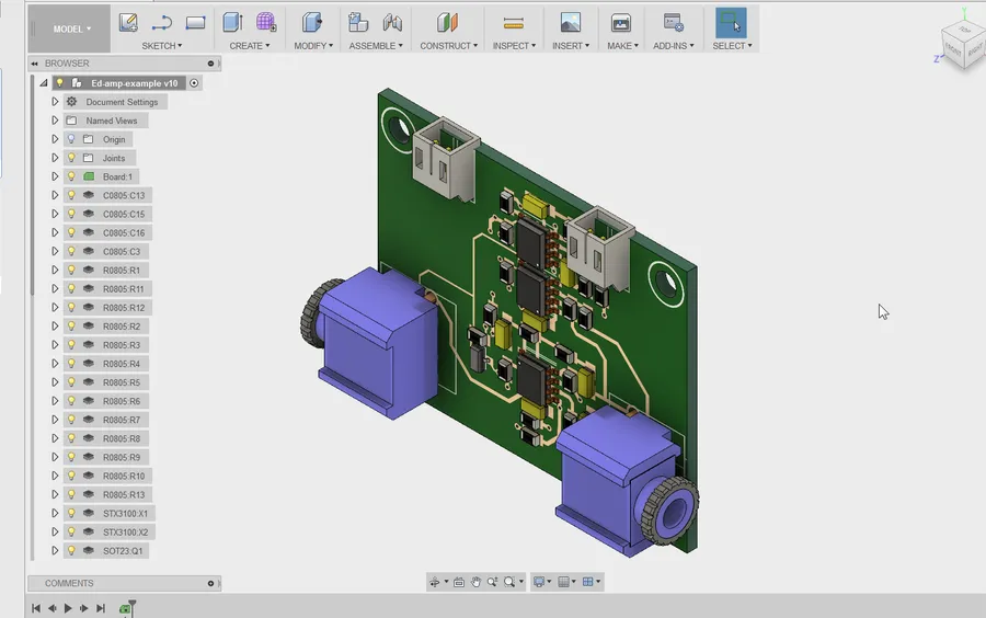
Effective PCB design hinges on selecting the right software and tools for schematic capture, layout design, and Gerber file generation. This section details several industry-standard software options and the importance of each design stage.
| Software | Description | Key Features | Pricing |
|---|---|---|---|
| Eagle | A widely-used PCB design tool known for its user-friendly interface and extensive component library. | Schematic capture, PCB layout, component library, 3D visualization | Subscription-based, free for personal use with limitations |
| KiCad | An open-source PCB design suite offering a full range of features, excellent for hobbyists and professionals. | Schematic capture, PCB layout, Gerber file generation, 3D viewer | Free and open-source |
| Altium Designer | A high-end PCB design tool favored by professional engineers for its advanced capabilities and data management. | Hierarchical schematic design, advanced routing, signal integrity analysis, team collaboration | Subscription-based, high cost |
| OrCAD | Another industry standard PCB design suite offering comprehensive tools for schematic capture and PCB layout. | Schematic capture, PCB layout, component library, signal integrity analysis, and 3D visualization. | Subscription-based, professional |
| EasyEDA | An online PCB design tool with a user-friendly interface and access to a large library of components. Integrates seamlessly with JLCPCB for ordering. | Schematic Capture, PCB Layout, Gerber File Generation, Cloud-Based, Component Library | Free with premium options for more storage/functionality |
The PCB design process is fundamentally divided into two key phases: schematic capture and layout design. Schematic capture involves drawing the electronic circuit using electronic symbols. The layout design takes this schematic information and translates it into a physical board layout. The design software is used to place components, route traces and define vias. Both these design phases are critical to ensure correct functionality of the PCB. Gerber files, an industry-standard format, are essential for PCB manufacturing as they contain all the information needed to fabricate the physical board.
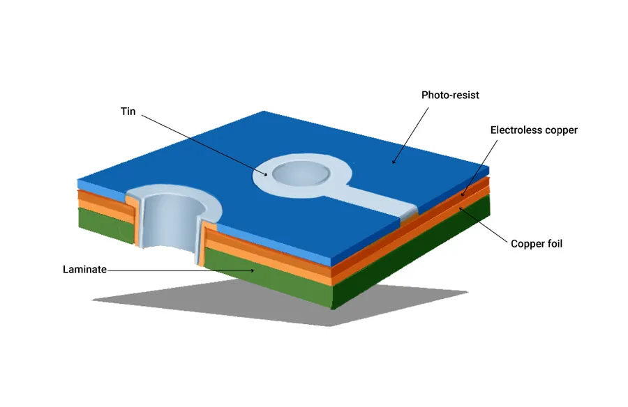
The fabrication of a Printed Circuit Board (PCB) is a multi-stage process that transforms a design into a physical, functional board. This process involves precision and control to ensure the final product meets the required specifications. From selecting raw materials to final testing, every step is crucial in determining the quality and reliability of the PCB.
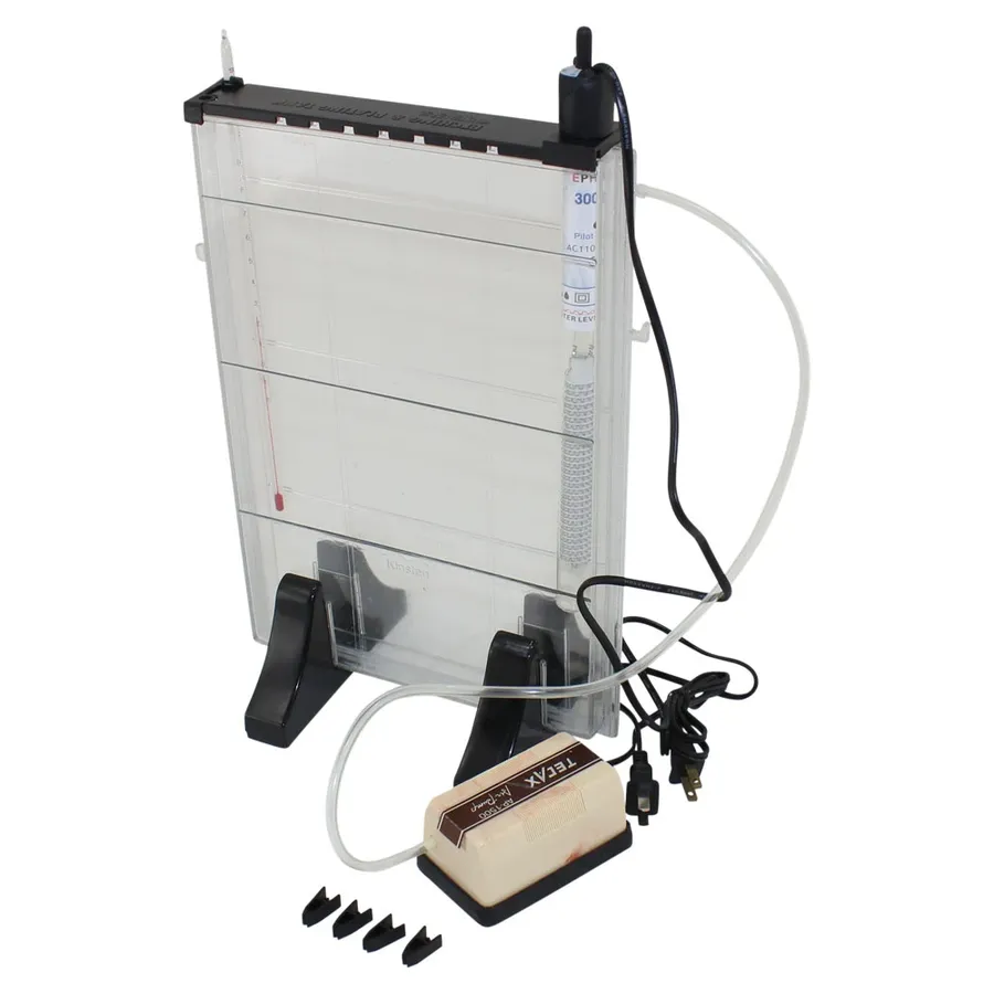
Creating printed circuit boards (PCBs) at home is a viable option for hobbyists and small-scale projects, allowing for rapid prototyping and customization. Several DIY methods are available, each with its own set of procedures, benefits, and limitations. These methods include toner transfer, photo-resist etching, and CNC milling, and each method varies in precision, cost, and complexity.
| Method | Process | Advantages | Disadvantages | Safety Precautions |
|---|---|---|---|---|
| Toner Transfer | Printing the PCB layout onto special paper, transferring toner to copper-clad board using heat, then etching. | Low cost, relatively simple, good for single-sided boards. | Can be inconsistent toner transfer, requires careful alignment, limited resolution. | Work in a well-ventilated area, use gloves, use caution with heat source. |
| Photo-Resist Method | Applying photo-sensitive film to the copper board, exposing it to UV light through a mask, developing, then etching. | Higher resolution than toner transfer, suitable for more complex designs, repeatable. | More steps involved, requires specific chemicals and UV exposure setup, can be more expensive. | Work in a dark room when applying the film, wear gloves, use proper ventilation when handling chemicals, use UV protection |
| CNC Milling | Using a CNC machine to directly remove copper from the PCB to create the traces. | High precision, allows for complex designs, can produce both single- and double-sided boards, no chemicals required. | High initial cost of the machine, requires specialized skills, can be slower than other methods. | Wear safety glasses, ensure proper machine operation, use dust collection system to avoid inhalation of micro particles |
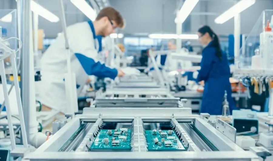
Professional PCB manufacturing services offer a significant leap in precision and quality compared to DIY methods, particularly when complex designs or larger production volumes are required. Outsourcing to specialized manufacturers like JLCPCB and PCBWay ensures adherence to strict industry standards, resulting in highly reliable and consistent circuit boards. This section explores the advantages and options available through professional PCB manufacturing.
| Feature | Professional PCB Manufacturing | DIY PCB Making |
|---|---|---|
| Precision | High (micron level) | Lower (millimeter level) |
| Quality | Consistent and High | Variable, Dependent on Skill |
| Complexity | Multi-layer, complex designs | Limited to Single or Double Layer |
| Volume | Suitable for both prototype and mass production | Suitable only for small batch production |
| Materials | Wide range of materials available | Limited Material Choice |
| Equipment | Advanced, Specialized machinery | Limited to basic tools and equipment |
| Cost | Cost-effective for large volumes, can be higher for prototypes | Lower upfront cost for small quantities |
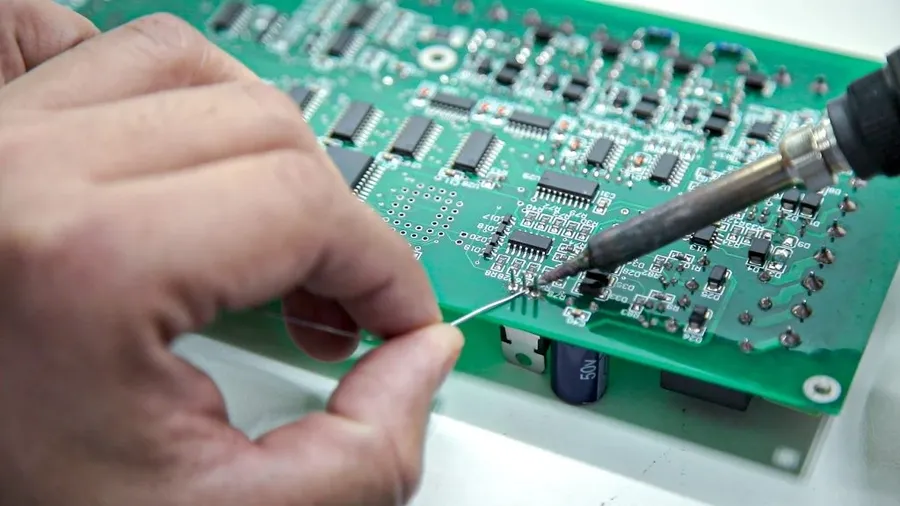
PCB assembly is the crucial process of populating a bare printed circuit board with electronic components, transforming it into a functional electronic device. This process can range from manual hand-soldering for prototypes to automated high-speed assembly for mass production, each with its own set of techniques and considerations.
Rigorous quality control and testing are paramount in PCB fabrication to ensure reliability and functionality. These steps are critical whether you're producing PCBs at home or outsourcing to a professional manufacturer. Effective testing catches defects early, preventing costly issues down the line and guaranteeing that the final product meets the required specifications.
The testing process often involves a combination of visual checks and sophisticated electrical tests, which verify both the physical integrity of the board and its electrical performance. From simple continuity checks to advanced automated optical inspections (AOI), a range of methods ensure every PCB meets standards.
| Testing Method | Description | Advantages | Disadvantages |
|---|---|---|---|
| Visual Inspection | Manual inspection of the PCB for visible defects such as misalignments, solder issues, and trace discontinuities. | Simple, low cost, and requires minimal equipment. | Subjective, can miss subtle defects, and is time-consuming for large volumes. |
| Continuity Testing | Checking electrical connections between different points on the PCB using a multimeter. | Quick and straightforward to verify basic connections. | Does not detect complex issues, and may not work with certain high-density designs. |
| Automated Optical Inspection (AOI) | Automated visual inspection that uses cameras to capture images and software to detect defects in solder joints, components, and alignment. | Highly accurate, fast, and consistent for large-scale PCB fabrication. | Requires investment in equipment, may have limitations with certain board types. |
| In-Circuit Testing (ICT) | Uses probes to test individual components and circuit nodes on the PCB, identifying shorts, opens, and component issues. | Comprehensive testing, can detect many types of electrical issues | Requires test fixtures and significant setup effort. |
| Functional Testing | Testing the complete functionality of the populated PCB under conditions that simulate real-world operations. | Verifies the correct operation of the entire circuit. | May require custom test setups, time-consuming, and may not cover all possible failure scenarios. |
Effective troubleshooting is crucial for successful PCB making, whether you're a hobbyist working at home or a professional in a manufacturing environment. This section addresses common issues that can arise during PCB fabrication and assembly and provides practical solutions to overcome these challenges, ensuring a functional final product.
This section addresses common inquiries regarding PCB (Printed Circuit Board) fabrication, encompassing both the overall process and specific techniques, to provide clarity on various aspects of PCB creation, from design to production.
Determining the most cost-effective method for PCB fabrication—whether through DIY techniques or professional manufacturing services—requires a detailed analysis of material costs, time investment, and equipment expenses. This section provides a comparative breakdown to aid in informed decision-making for your PCB project.
| Cost Factor | Home PCB Making (DIY) | Professional PCB Manufacturing |
|---|---|---|
| Materials (e.g., copper clad boards, chemicals, etching solutions) | Low for basic setups, but increases with complexity and quality requirements. | Cost-effective at scale due to bulk purchasing and efficient processes. |
| Equipment (e.g., UV exposure box, etching tanks, drilling machines, soldering station) | Can be minimal for very basic methods, but significantly increases for higher accuracy and more complex designs. initial equipment costs can be high. | Included in service cost; no initial investment needed for production equipment. |
| Time Investment | High; Requires significant time for design, setup, fabrication, and rework. | Lower; Production time can vary from a few days to a couple weeks based on complexity and order size. Standard turnaround time is usually consistent and fast. |
| Labor Cost | High if valuing your time. Time spent is usually not quantified. | Included in service cost; efficient automated assembly processes. |
| Accuracy & Reliability | Highly dependent on skill and equipment; results can be inconsistent or unreliable. | High accuracy and reliability due to precision machinery and quality control. |
| Setup Costs | Potentially lower for very simple single-sided board but can increase when doing double sided board or more complex board with plated through holes. Multiple attempts may require additional expenses. | Minimal set up costs for simple boards with standard requirements. |
| Volume Production | Difficult and time-consuming to produce multiple copies. | Designed for efficient mass production at a reduced per-unit cost. |
| Complexity Handling | Limited by equipment, skills, and material. Difficult to do multi layer boards. | Capable of handling complex multi-layer PCBs, fine pitch components and specialized requirements. |
| Waste & Environmental Impact | Chemical usage may lead to increased waste if not controlled properly. | Professional service have environmental control and are likely more sustainable. |
Ultimately, the choice between home and professional PCB fabrication hinges on project requirements and resource availability. For simple prototypes or hobbyist projects, DIY methods can be educational and cost-effective, but when precision, reliability, and volume are needed professional manufacturing is a more efficient and economical choice.
Mastering the art of PCB making is a rewarding journey, whether for a simple hobby project or a complex professional undertaking. This comprehensive guide has walked you through every step, from design to final assembly, empowering you to create your own custom electronic circuits. Whether you choose a DIY approach or opt for professional services, understanding the intricacies of PCB making is essential for successful electronics projects. Continue to explore and experiment, and you'll find yourself at the forefront of innovation in the fascinating world of PCB making.

