Just as a water faucet controls the flow of water, a transistor, a fundamental building block of modern electronics, controls the flow of electrical current. At the heart of this tiny switch lies three key components: the emitter, the base, and the collector. These parts, like the valve, handle, and output of a faucet, each play a crucial role in the transistor’s operation. Understanding these parts is essential to grasping how transistors, and therefore many electronic devices, work, from your smartphone to the most complex computer processors. This article will delve into these core components, explaining their function and importance.
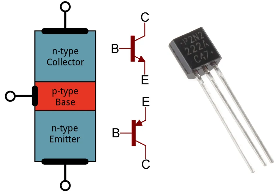
The emitter, a crucial component of a transistor, serves as the source of charge carriers—either electrons in NPN transistors or holes in PNP transistors—which are injected into the base region. Functionally analogous to a water faucet's source, it initiates the flow of charge necessary for transistor operation. To ensure a substantial and consistent supply of charge carriers, the emitter is heavily doped.
| Characteristic | Description |
|---|---|
| Function | Supplies charge carriers (electrons or holes) into the base region. |
| Analogy | Source of water in a faucet, providing the initial flow. |
| Doping | Heavily doped to ensure a substantial supply of charge carriers. |
| Charge Type(NPN) | Electrons are emitted. |
| Charge Type(PNP) | Holes are emitted. |
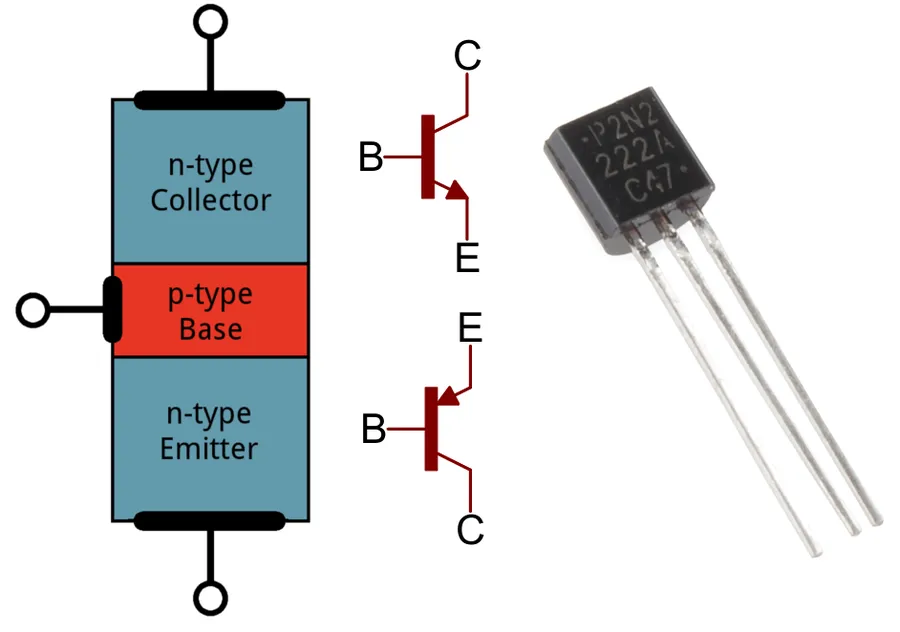
The base of a transistor functions as a control valve, meticulously regulating the flow of charge carriers—either electrons in NPN transistors or holes in PNP transistors—from the emitter towards the collector. Its key characteristic is its ability to modulate a significant current between the emitter and collector with a comparatively small input signal. This delicate control is pivotal for both amplification and switching functionalities, requiring the base region to be extremely thin and precisely fabricated.
The base's importance lies in its ability to act as a gatekeeper, allowing or restricting the current flow between the emitter and collector. A minimal current or voltage applied to the base terminal can cause a considerable shift in the current flow, making it a key component in electronic devices requiring signal amplification or rapid switching actions. This precise regulation is achieved through the base's design and material properties.
The design of the base region is crucial for its function. A very thin layer is typically used to minimize the transit time for charge carriers and maximize the efficiency of the transistor. The doping concentration in the base region is also carefully controlled to optimize the current flow and minimize any parasitic effects. The base must be precisely manufactured to ensure reliable and consistent operation of the transistor.
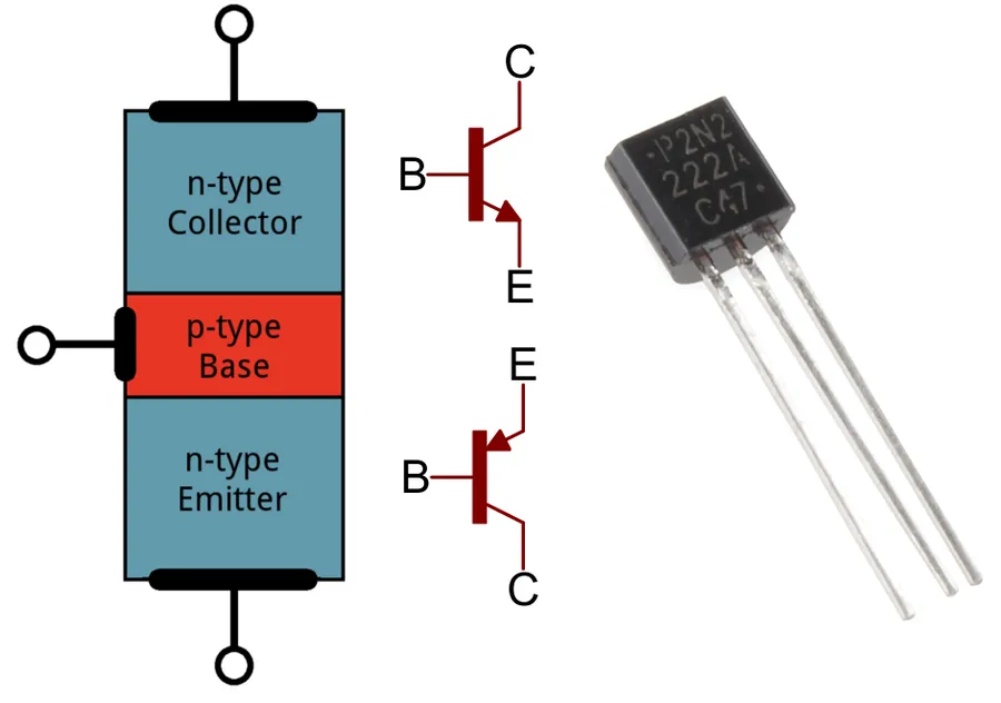
The collector is a crucial part of a transistor, acting as the terminal that receives charge carriers—either electrons or holes—after they have traversed the base region. Functioning as the 'output' terminal, it is responsible for collecting and carrying away the regulated current that the transistor manipulates. The design and size of the collector are critical, especially in terms of heat management, as it is here where a significant amount of power can be dissipated.
| Feature | Description |
|---|---|
| Function | Receives charge carriers from the base, acting as output terminal. |
| Charge Type | Receives either electrons (in NPN transistors) or holes (in PNP transistors). |
| Design Importance | Optimized for efficient charge collection and heat dissipation. |
| Placement | Positioned to complete the current path from emitter, through the base. |
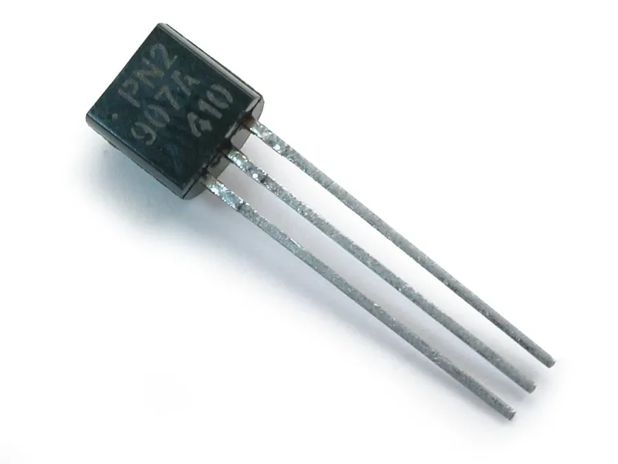
Transistors are broadly classified into two main types: NPN and PNP. These classifications are based on the arrangement and doping of the semiconductor materials within the emitter, base, and collector regions, which fundamentally dictate their operational characteristics. Understanding these differences is crucial for effective circuit design.
| Feature | NPN Transistor | PNP Transistor |
|---|---|---|
| Majority Charge Carriers in Emitter | Electrons | Holes |
| Polarity of Voltage between Base and Emitter (Active Region) | Positive | Negative |
| Direction of Conventional Current Flow | Emitter to Collector | Collector to Emitter |
| Doping Arrangement | N-type Emitter, P-type Base, N-type Collector | P-type Emitter, N-type Base, P-type Collector |
| Base Current Flow | Into the base | Out of the base |
In NPN transistors, the emitter region is heavily doped with N-type material, releasing electrons into the base region, while the collector region, also N-type, collects these electrons. The base region is P-type and relatively thin. Conversely, PNP transistors feature a P-type emitter that injects holes into the N-type base, which then flow to the P-type collector. The voltage polarities required for active operation are opposite between these two types. The operational principle remains that the base current controls the flow of majority carriers (electrons in NPN, holes in PNP) between the emitter and collector, but the direction of current and voltage polarity in the circuit design is reversed. The selection between NPN and PNP transistors in circuit design depends on the desired functionality and voltage requirements, each offering unique advantages in different applications.
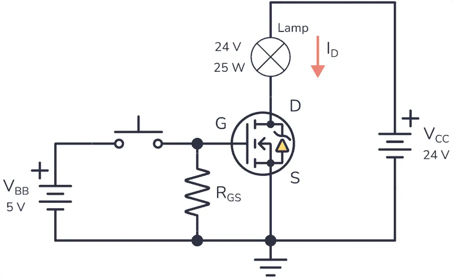
Transistors, at their core, function as electronic switches, with the base controlling the current flow between the emitter and collector. This switching capability stems from the interaction of the three terminals and their unique doping characteristics. A small change in voltage or current at the base can produce a significant change in the current flow through the transistor, effectively turning it 'on' or 'off'.
In an NPN transistor, a small positive voltage applied to the base relative to the emitter allows electrons to flow from the emitter, through the base, and into the collector, completing the circuit and allowing current to flow. Conversely, if the base voltage is lowered (or zero), the electron flow is reduced to almost zero, effectively turning off the switch. For a PNP transistor the principle is the same but is operating with holes as charge carriers and the biasing voltage is of opposite polarity.
| Transistor Type | Switching State | Base Condition | Emitter-Collector Current Flow |
|---|---|---|---|
| NPN | On | Sufficiently positive voltage on base (relative to emitter) | Significant current flow |
| NPN | Off | Insufficient positive voltage on base (or close to zero) | Minimal current flow |
| PNP | On | Sufficiently negative voltage on base (relative to emitter) | Significant current flow |
| PNP | Off | Insufficient negative voltage on base (or close to zero) | Minimal current flow |
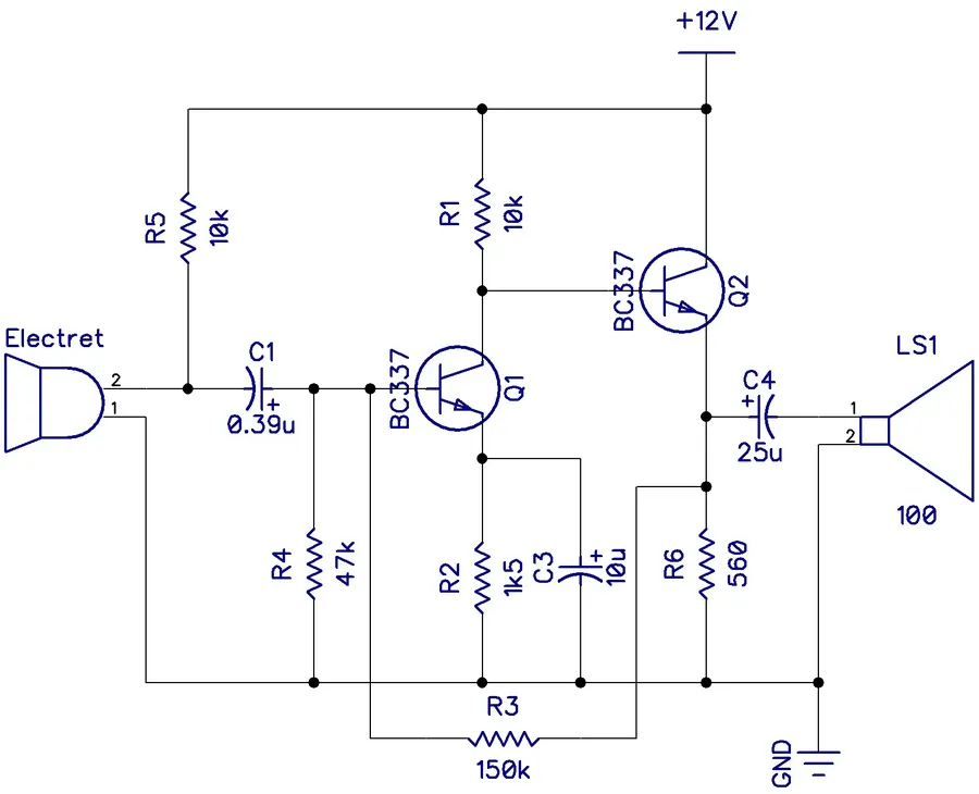
Transistors, leveraging the interplay between their emitter, base, and collector, are fundamental to signal amplification. This crucial function allows transistors to increase the power of a weak electrical signal, making it useful in a wide array of electronic applications. The key to this amplification lies in the transistor's ability to control a larger current flow between the emitter and collector with a much smaller current or voltage applied to the base.
In amplification, a small input signal applied to the base modulates the larger current flowing from the emitter to the collector. This modulation mirrors the shape and characteristics of the input signal but with significantly increased magnitude. This ability to replicate and magnify the signal forms the basis for audio amplifiers, radio receivers, and various other electronic devices.
| Transistor Part | Role in Amplification | Analogy |
|---|---|---|
| Emitter | Provides the initial charge carriers. | Source of water in a faucet. |
| Base | Controls the flow of charge carriers from emitter to collector, modulating current based on input signal. | Control valve that modulates water flow based on lever input. |
| Collector | Receives and outputs the amplified charge carriers. | Destination where the water flows out. |
By fine-tuning the circuit parameters, engineers can precisely control the amount of amplification provided by a transistor. This capability to manipulate signal strength and shape is essential in many electronic devices, ensuring reliable operation.
This section addresses common questions about the components of transistors, clarifying their roles and functionalities. We will explore the emitter, base, and collector, alongside fundamental aspects like transistor structure and pin configurations.
Accurately identifying the emitter, base, and collector pins of a transistor is crucial for circuit design and troubleshooting. This section provides practical methods for pin identification using datasheets, multimeters, and visual inspection techniques.
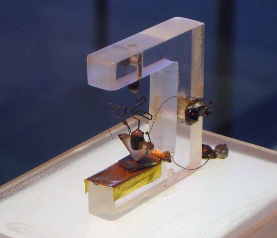
The trajectory of transistor technology has been marked by continuous innovation in materials science and manufacturing techniques, leading to significant advancements in miniaturization, efficiency, and performance. This evolution has been the cornerstone of modern electronics, profoundly impacting various aspects of our lives, while still operating on the core principles of emitter, base and collector control.
Early transistors were relatively large and less efficient, often constructed from germanium. However, the transition to silicon as the primary semiconductor material revolutionized the industry. Silicon's superior temperature stability and abundance enabled the production of smaller, more reliable devices.
Advancements in photolithography and etching processes allowed for the creation of increasingly complex integrated circuits (ICs) containing millions, and now billions, of transistors on a single chip. These developments have driven down costs, increased performance, and facilitated the development of powerful but compact devices.
Moreover, the introduction of novel materials, like gallium arsenide, has enabled the fabrication of high-speed transistors for specialized applications. Additionally, research continues into new transistor structures, like FinFETs and nanowire transistors, that enhance performance and reduce power consumption.
The principles of emitter, base, and collector control, however, remain fundamental to the operation of all transistors, regardless of their size or material. The remarkable progress made in miniaturizing and enhancing transistor technology shows how scientific breakthroughs coupled with manufacturing advancements has resulted in modern microelectronics, all starting from simple and early designs.
The transistor's humble parts - the emitter, the base, and the collector - are not merely components; they are the gatekeepers of modern technology. Like the interplay of the faucet, these components enable precise control over electrical current, powering our digital world. This basic unit and the relationships between its parts is the cornerstone of everything from simple circuit design to advanced microprocessors. Understanding the function of these crucial parts of a transistor allows you to understand the very essence of how modern electronics work, and provides a basis for innovation in the future.

