Understanding PCB: From Basics to Advanced Applications
2025.02.02
The printed circuit board (PCB) is the unsung hero of modern electronics. From the smartphones in our pockets to the complex machinery of industrial robots, PCBs are the foundation upon which nearly every electronic device is built. Understanding what a PCB is, how it's designed, and its various applications is crucial in our technologically driven world.
What is a PCB?
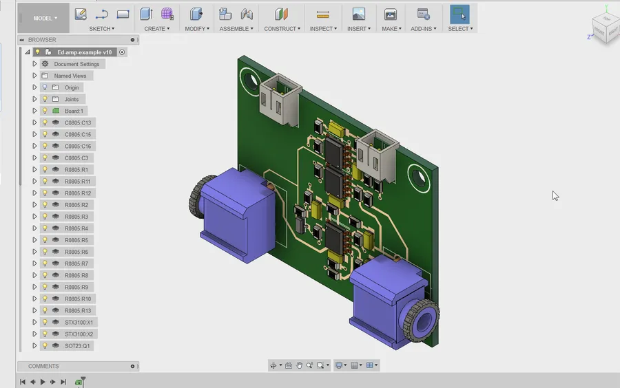
Printed Circuit Board
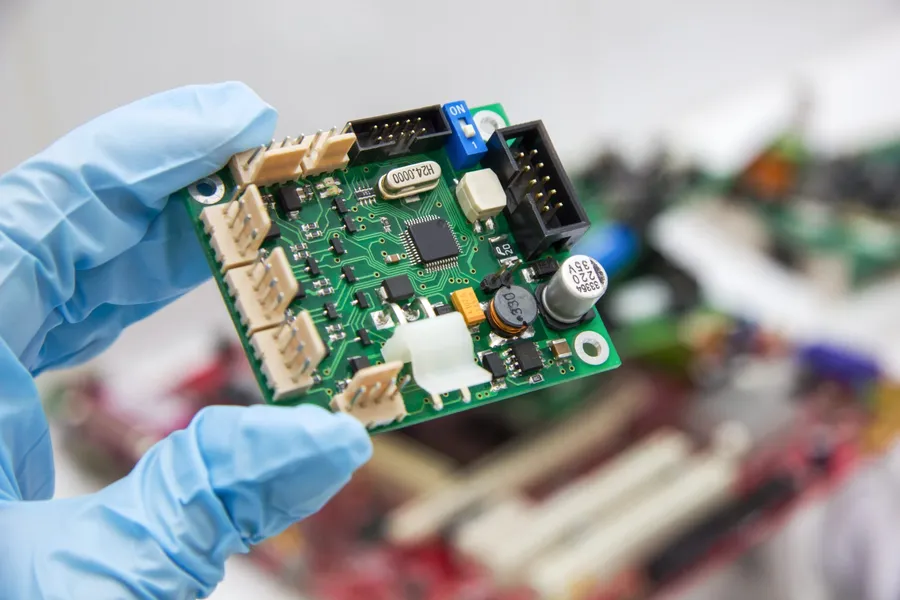
A printed circuit board (PCB), or printed wiring board (PWB), fundamentally serves as the foundational structure for nearly all electronic devices. It's a non-conductive substrate, typically made of fiberglass, upon which conductive pathways, typically copper, are etched or laminated to interconnect electronic components. The PCB provides both mechanical support and the necessary electrical pathways for components to function within a circuit.
Non-Conductive Substrate The base material of a PCB, often fiberglass epoxy resin (FR-4), provides insulation and structural integrity.
Conductive Pathways Copper traces etched onto the substrate provide low-resistance paths for electrical current between components.
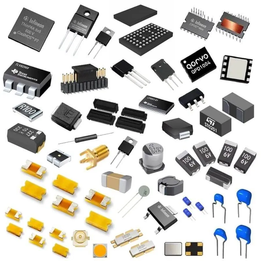
Component Mounting The PCB design includes pads and mounting features for attaching electronic components such as resistors, capacitors, and integrated circuits.
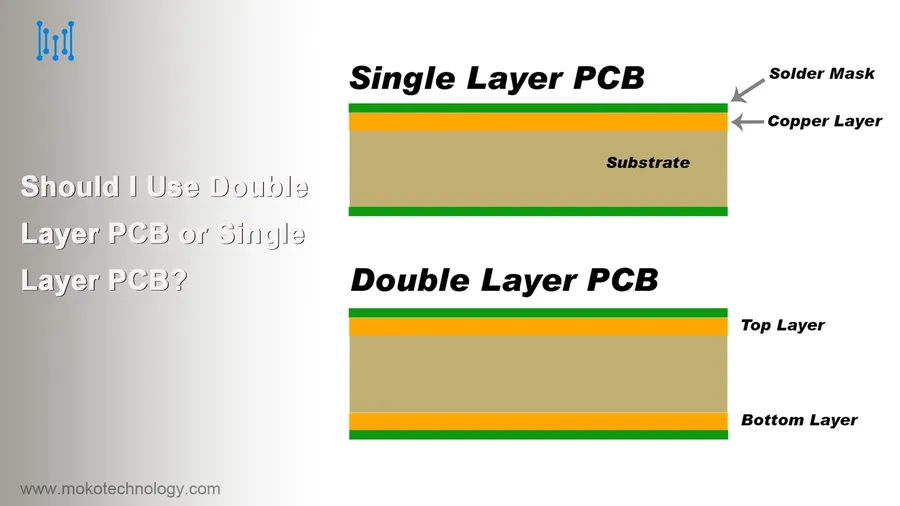
Layered Construction PCBs can be single-layer, double-layer, or multi-layer, depending on the circuit complexity and density requirements.
Feature
Description
Substrate
Provides mechanical support and electrical insulation, typically FR-4 or similar material.
Copper Traces
Conductive pathways for electrical current, usually made of copper.
Pads
Areas of exposed copper for soldering components.
Vias
Holes plated with copper that enable electrical connections between layers of a multi-layer PCB.
PCB Manufacturing Process
PCB Manufacturing Stages
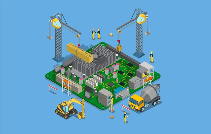
The manufacturing of a Printed Circuit Board (PCB) is a sophisticated process involving multiple stages, each critical to the final product's functionality and reliability. This process transforms a conceptual electronic design into a physical, functional circuit board.
Design and Layout The process begins with a detailed electronic schematic and layout using CAD software. This phase defines the electrical connections, component placement, and overall board structure.
Material Selection Appropriate substrate materials, typically fiberglass reinforced epoxy resin (FR-4), are chosen based on performance requirements, such as thermal and electrical properties. Copper is used for conductive traces, and the thickness is determined by the current-carrying requirements.
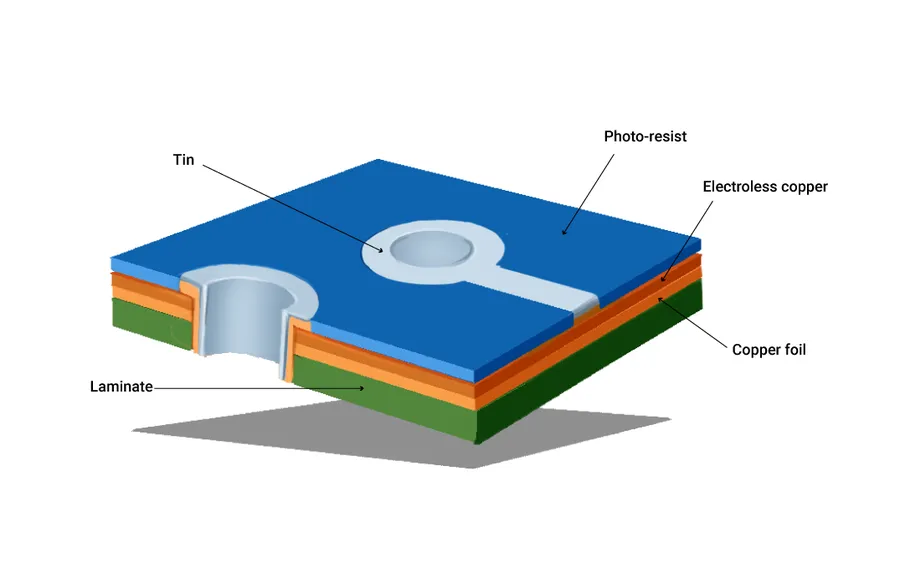
Image Transfer A negative image of the circuit layout is transferred onto a copper clad laminate board through photo-imaging processes. This is achieved by coating the board with a light sensitive material (photoresist) then exposing it to UV light through the circuit design pattern, hardening the desired circuit pattern.
Etching The unexposed photoresist is removed with chemical solutions, and the unwanted copper is etched away, leaving behind the required circuit traces. The hardened photoresist protects the desired copper pattern.
Drilling Holes for component leads and vias (interlayer connections) are precision-drilled using numerically controlled machines. This ensures accurate component placement and reliable electrical connections.
Plating After drilling, the hole walls are plated with copper to form reliable electrical connections. This involves a series of chemical baths and deposition processes. Additional plating with tin or other metals may be done to aid in soldering.
Solder Mask Application A solder mask (protective coating), usually a polymer, is applied to the board to prevent solder bridging between traces. This coating ensures that solder only adheres to the designated pads, facilitating precise component assembly.
Silkscreen Printing A silkscreen (legend) of component designators, reference points, or identification marks is added using ink. This allows easier assembly of the electronic components and provides critical test points.
Surface Finish Various surface finishes are applied to the exposed copper pads to protect them from oxidation and improve solderability. These can include HASL, ENIG, or immersion tin, among others. The choice is dependent on the solder material and performance requirements.
Electrical Testing Bare boards are tested for continuity, shorts, and isolation using automated test equipment to ensure that all traces and connections are functional as per design. This ensures that any defects are caught before component assembly.
Profiling The individual PCBs are cut out of the panel according to the specifications using routing or laser cutting technologies. At the end of the process, the boards are inspected, cleaned, and then prepared for the next stage: component assembly.
Manufacturing Step
Purpose
Key Technologies
Design & Layout
Define circuit connections and component placements
CAD Software
Material Selection
Choose appropriate substrate and conductive materials
Material Science, Supplier Catalogs
Image Transfer
Transfer circuit design onto the board
Photo-imaging, UV light
Etching
Remove unwanted copper to create circuit traces
Chemical Etchants
Drilling
Create holes for component leads and vias
CNC Machines
Plating
Deposit conductive material in holes and on surfaces
Electroless Plating
Solder Masking
Apply a protective layer to prevent solder bridging
Screen Printing, UV Curing
Silkscreen Printing
Add component designators and labels
Ink Printing
Surface Finish
Protect copper pads and enhance solderability
Immersion Baths, Plating
Electrical Testing
Verify the integrity of the circuit board
Automated Testing Equipment
Profiling
Cut individual PCBs from the production panel
Routing, Laser Cutting
Types of PCBs: Single-Layer, Double-Layer, and Multilayer
PCB Layer Comparison
Printed circuit boards are manufactured in several configurations, primarily distinguished by the number of conductive layers: single-layer, double-layer, and multilayer. The choice of PCB type is contingent on the application's complexity, component density, and performance demands. Each type offers unique advantages and disadvantages.
PCB Type
Description
Typical Applications
Advantages
Disadvantages
Single-Layer
Has one conductive layer, typically copper, on one side of the substrate.
Simple electronics, toys, basic lighting circuits
Lowest cost, simplest design, easy to manufacture
Limited component density, cannot support complex circuits
Double-Layer
Has conductive layers on both sides of the substrate.
Consumer electronics, power supplies, basic communication devices
Increased component density, more complex routing, relatively low cost
More difficult to manufacture than single layer PCBs, limited routing space compared to multilayer
Multilayer
Has three or more conductive layers separated by insulating material.
Advanced electronics, high-speed data processing, aerospace, medical equipment
High component density, very complex routing, optimal performance
Highest cost, most complex design, challenging to manufacture
Multilayer PCBs, with their multiple conductive layers, provide enhanced capabilities for complex electronic systems. The increased number of layers allows for intricate routing of signals and facilitates denser component placement. This is essential for miniaturization and high-performance applications, making multi-layer boards crucial in cutting-edge technologies.
Key Components of a PCB
PCB Components
Printed Circuit Boards (PCBs) are comprised of several key components that facilitate their functionality. These components include conductive traces for electrical pathways, pads for component soldering, vias for interlayer connections, and the substrate material, commonly fiberglass. The precise arrangement and quality of these elements are crucial for ensuring proper electrical flow and circuit performance, which is the backbone for modern electronics.
Conductive Traces These are copper pathways etched onto the PCB substrate, facilitating the flow of electrical current between components. Their width and thickness are designed based on the current they need to carry, and signal integrity requirements.
Pads Pads are small, exposed metal areas on the PCB where electronic components are soldered. They come in various shapes and sizes, depending on the type of component to be mounted, and are critical for creating a stable and reliable electrical connection.
Vias Vias are plated through-holes that create electrical connections between different layers of a multi-layer PCB. They are crucial for enabling complex routing and maintaining signal integrity in compact designs.
Substrate Material The substrate, typically made of fiberglass reinforced epoxy (FR-4), provides the base for the PCB. It is a non-conductive material that supports the conductive layers and provides mechanical strength. Other materials like ceramic or flexible polymers may be used for specialized applications.
Solder Mask This is a thin layer of polymer that protects the conductive traces from oxidation and prevents solder bridges during the assembly process. It leaves only the pads exposed for soldering components.
Silkscreen The silkscreen is a layer of ink printed on the PCB surface that provides reference designators, component locations, and other useful information for assembly and debugging.
Component
Function
Material
Importance
Conductive Traces
Electrical Pathways
Copper
Ensures proper signal transmission.
Pads
Soldering points for components
Copper (plated)
Provides stable mounting and connection.
Vias
Interlayer electrical connection
Plated through holes
Facilitates complex circuit layouts.
Substrate
Base structure
Fiberglass (FR-4), ceramic
Provides mechanical support and insulation.
PCB Design Considerations
PCB Design Software
Effective PCB design is paramount for ensuring optimal circuit functionality, involving a multi-faceted approach that addresses signal integrity, thermal management, impedance matching, and component placement. These considerations are critical for high-performance and reliable electronic devices, and must be carefully managed through planning and simulation.
Signal Integrity Signal integrity ensures that electrical signals maintain their intended form and strength as they travel through the PCB. This involves minimizing signal reflections, crosstalk, and noise to prevent data corruption and signal degradation.
Thermal Management Efficient thermal management is essential to prevent overheating of components. Adequate heat dissipation techniques, such as heatsinks, thermal vias, and appropriate component placement, help maintain safe operating temperatures for all components.
Impedance Matching Impedance matching optimizes the transfer of power between components. It involves designing transmission lines on the PCB with specific impedance values to minimize signal reflections and maximize power transfer.
Component Placement Careful component placement reduces electrical noise and thermal issues and must consider factors such as proximity to other components and the overall layout of the circuit.
PCB design software, such as Altium Designer, Cadence Allegro, or KiCad, allows engineers to simulate these factors and optimize the layout of the board before manufacturing. The use of such tools enables engineers to predict and rectify potential design flaws, ensuring that the final product performs as expected.
PCB Applications Across Industries
Automotive PCB
Printed circuit boards (PCBs) are fundamental components in nearly all modern electronic devices, demonstrating their broad applicability across diverse industries. Their versatility stems from their ability to provide a stable platform for mounting and interconnecting electronic components, thus enabling a wide range of functions.
The following table outlines key applications of PCBs across various sectors:
Facilitate precise measurement, control, and communication required for diagnostic, monitoring, and therapeutic applications.
Industrial Automation
Programmable logic controllers (PLCs), industrial robots, process control systems, sensors and transducers
Enable automation, monitoring, and control of industrial processes, ensuring efficiency and productivity.
Telecommunications
Network switches, routers, base stations, mobile communication devices
Enable transmission, routing, and processing of data for voice, data, and video communication.
Renewable Energy
Solar inverters, wind turbine controllers, battery management systems
Enable efficient energy conversion, storage, and distribution for sustainable energy solutions.
The continued evolution and improvement in PCB technology is driving advancements in many technological fields. The use of advanced materials and manufacturing techniques enables the creation of smaller, more powerful, and more reliable electronic devices.
PCB Assembly and Testing
The process of assembling and testing a printed circuit board (PCB) is crucial to ensure its functionality and reliability. This stage follows PCB fabrication and involves mounting electronic components onto the board, followed by rigorous testing to confirm design specifications and performance.
Surface Mount Technology (SMT) SMT is a method for mounting electronic components directly onto the surface of a PCB. SMT components are typically smaller and more compact than through-hole components, allowing for higher component density and smaller board sizes. This method is widely used for mass production due to its efficiency and automation capabilities.
Through-Hole Technology Through-hole technology involves inserting component leads through holes drilled in the PCB and soldering them on the opposite side. This method is often used for larger components and for connections that require higher mechanical strength. Although less common in mass production now, through-hole remains essential in prototyping and specialized applications.
Soldering Techniques Both SMT and through-hole technologies require precise soldering to ensure electrical connections between the components and the PCB. Soldering can be done manually or automated, depending on the volume of production and component type. Common soldering methods include reflow soldering for SMT, and wave soldering for through-hole components.
Post-assembly, PCBs undergo comprehensive testing to verify proper functionality. Testing includes both electrical and functional tests.
In-Circuit Testing (ICT) ICT is used to check for manufacturing defects such as shorts, opens, and incorrect component values before a circuit is powered on. This test involves using probes that make contact with test points to check each component's connectivity and proper placement. It's an essential part of ensuring high product reliability.
Functional Testing Functional testing involves powering up the PCB and testing its performance under various operating conditions. This test validates whether the PCB performs the functionality for which it was designed and it ensures that the entire circuit is operating within the expected specifications. Functional testing methods depend on the complexity of the PCB and its intended application.
Automated Optical Inspection (AOI) AOI is used for automatically inspecting the assembled PCBs for any assembly defects, such as missing components, misaligned parts, or poor solder joints. AOI uses cameras to capture high-resolution images, comparing them to a reference image to identify errors, enhancing the speed and precision of the testing process.
The combination of careful assembly and rigorous testing ensures that PCBs meet performance and reliability standards, thus preventing failures in the field and reducing the need for expensive field repairs.
Frequently Asked Questions about PCBs
This section addresses common queries about PCBs, providing concise answers to frequently asked questions. These answers are based on fundamental principles and aim to provide clear, technically accurate information.
What does PCB stand for, and what is its fundamental role? PCB stands for Printed Circuit Board. Its primary role is to provide a structural base and conductive pathways for electronic components, forming the foundation of nearly all modern electronics.
What are the primary applications of PCBs across different industries? PCBs are integral to almost every electronic device, including smartphones, automotive systems, medical equipment, aerospace technology, and industrial control systems. They serve as the core structure for mounting and interconnecting components.
What is the full form of PCB? The full form of PCB is Printed Circuit Board. The name highlights its core feature: a board where circuits are printed using conductive traces.
What are common PCB design tools used in the industry? Commonly used PCB design tools include Altium Designer, Cadence Allegro, Eagle, and KiCad. These tools offer features for schematic capture, PCB layout, and simulation.
What are the main types of PCBs, and what is their primary difference? The main types of PCBs include single-sided, double-sided, and multilayer boards. Single-sided boards have conductive pathways on one side, double-sided have them on both, and multi-layer boards have multiple layers, increasing circuit complexity and component density.
What environmental concerns are associated with PCBs, and how are they addressed? PCBs can contain hazardous materials like lead, posing environmental risks. The best way to address this is through responsible recycling, using lead-free components, and employing eco-friendly manufacturing processes to minimize their impact.
What is the difference between SMT and through-hole component mounting on a PCB? Surface Mount Technology (SMT) involves mounting components directly on the surface of the PCB, while through-hole mounting involves inserting component leads through holes in the PCB and soldering them on the opposite side. SMT is generally used for smaller components and higher density designs.
Environmental Concerns and PCB Disposal
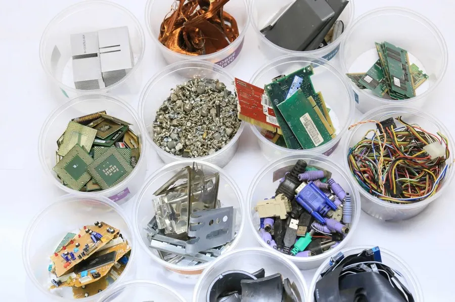
PCB Recycling
The widespread use of PCBs, while essential for modern electronics, presents significant environmental challenges due to the presence of hazardous materials such as lead, brominated flame retardants, and other toxic substances. These materials can leach into the environment, contaminating soil and water, and pose risks to human health and ecosystems if not managed responsibly. Proper disposal and recycling are critical to mitigate these adverse effects.
Hazardous Materials in PCBs PCBs contain various hazardous materials, including heavy metals (such as lead and cadmium), brominated flame retardants (BFRs), and other persistent organic pollutants (POPs). These substances can cause environmental pollution and pose health risks.
Environmental Impact Improper disposal of PCBs leads to soil and water contamination. Heavy metals and POPs can accumulate in the food chain, affecting wildlife and eventually humans. E-waste, which often contains PCBs, is a significant source of pollution.
Health Risks Exposure to hazardous materials from PCBs can lead to various health issues, including neurological disorders, reproductive problems, and increased cancer risks. Workers in e-waste processing facilities are particularly at risk if proper safety measures are not in place.
Responsible Disposal Practices Effective PCB disposal requires specialized recycling and treatment processes. This includes dismantling and separating components and ensuring safe removal and management of hazardous substances. Incineration at high temperatures under controlled conditions may be necessary for some PCB waste.
Eco-friendly Manufacturing Methods Moving towards eco-friendly manufacturing reduces the environmental impact of PCBs. This can involve using alternative materials and processes that minimize toxic waste and energy consumption, with an emphasis on reducing material waste.
Recycling and Reuse Recycling is important, but extracting reusable materials from PCBs is technically challenging and requires specialized facilities. Reuse of components and materials, when possible, can reduce the need for new resources and the amount of PCB waste generated.
Regulatory Compliance Compliance with international and national regulations related to hazardous materials and e-waste is essential for managing PCBs properly. This helps to ensure the safe handling, transportation, and disposal of PCBs, thereby protecting the environment and public health.
In conclusion, PCBs are the foundational technology behind the vast majority of electronics today. From their design and manufacturing process, to their many applications, their role in society cannot be overstated. Understanding PCBs is crucial to appreciating our increasingly technology-driven world and driving future innovation. With ongoing advancements in manufacturing and environmental responsibility, the future of PCBs is set to continue shaping the landscape of technology.