Transistors, the unsung heroes of modern electronics, are fundamental to everything from your smartphone to the most advanced supercomputers. Understanding a transistor's role begins with interpreting its schematic symbol, a kind of visual language for electronic circuits. This article delves into the world of transistor schematics, exploring their components, types, and practical uses, and includes a [transistor schematic]. Think of it as the blueprint that allows engineers to orchestrate the flow of electricity, creating the technology we rely on daily. This article will help you read those blueprints.
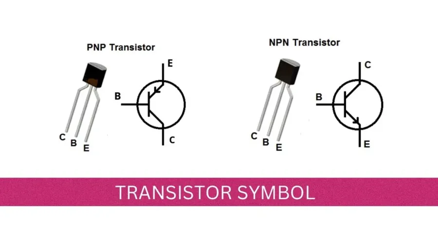
The cornerstone of understanding any transistor circuit lies in the ability to decipher its schematic representation. This section focuses on the fundamental transistor symbol, dissecting its components—the base, collector, and emitter—as depicted in both NPN and PNP configurations. Accurate identification of these elements is crucial for analyzing circuit behavior and troubleshooting.
A transistor, at its core, is a three-terminal semiconductor device used to amplify or switch electronic signals and electrical power. The schematic symbol abstracts this complex device into a recognizable form. Key to understanding is the correct identification of the three terminals: the Base (B), Collector (C), and Emitter (E), and to differentiate between NPN and PNP types.
In the schematic, the transistor symbol varies slightly depending on whether it is an NPN or a PNP type. The primary difference is the direction of the arrow on the emitter terminal. For an NPN transistor, the arrow points *away* from the base, indicating the direction of conventional current flow when the transistor is active. Conversely, in a PNP transistor, the arrow points *toward* the base. This seemingly small detail is critical for determining the bias conditions and the overall function of the transistor within the circuit.
| Feature | NPN Transistor | PNP Transistor |
|---|---|---|
| Arrow Direction on Emitter | Points Away from Base | Points Towards Base |
| Conventional Current Flow | Collector to Emitter | Emitter to Collector |
By carefully examining the transistor symbol and its orientation in a circuit schematic, it's possible to discern the type of transistor (NPN or PNP), the direction of current flow under various operating conditions, and the role the transistor plays in that specific circuit design. This ability is the foundational element for understanding more complex schematics and circuit analysis.
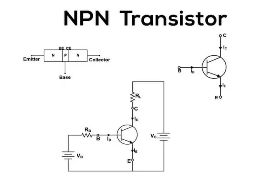
The NPN transistor, a cornerstone of modern electronics, is characterized by its specific schematic representation which is crucial for understanding its function within a circuit. The NPN transistor schematic clearly illustrates the direction of current flow, which is conventionally depicted from the collector to the emitter when the base is activated. This arrangement highlights its role as a current-controlled switch or amplifier.
| Component | Symbol | Function |
|---|---|---|
| Collector (C) | Arrow points towards the transistor body | Terminal where current enters from the power supply |
| Base (B) | A small input pin perpendicular to the emitter and collector | Control terminal that regulates current flow |
| Emitter (E) | Arrow points away from the transistor body | Terminal where current exits towards ground or another circuit element |
In an NPN transistor schematic, the direction of the arrow on the emitter terminal always indicates the conventional current flow direction for positive charges. For the NPN transistor, this arrow always points *away* from the transistor body (or toward the ground). Understanding this directionality is paramount for circuit analysis, as it dictates the biasing requirements and overall operation.
When the base is provided with a positive voltage relative to the emitter, it allows current to flow from the collector to the emitter. This characteristic is fundamental to the NPN transistor’s operation as an electronic switch or a signal amplifier. Different resistor or capacitor values connected to the base will change how the transistor operates. By using the NPN's gain characteristics, a small current flowing into the base of the transistor allows for a much larger current to flow through the collector and emitter. This characteristic allows the NPN transistor to act as both a switch or an amplifier.
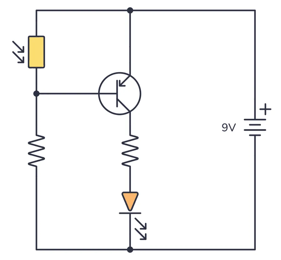
While NPN transistors are more commonly encountered, understanding PNP transistor schematics is crucial for comprehending a wide array of circuit designs. The key distinction lies in the direction of current flow and the polarity of voltage required to activate the transistor. This section elucidates these differences, enabling engineers and students to interpret both NPN and PNP transistor schematics effectively.
| Feature | NPN Transistor | PNP Transistor |
|---|---|---|
| Current Flow | Current flows from collector to emitter. | Current flows from emitter to collector. |
| Biasing Voltage | Base voltage is higher than emitter voltage to turn the transistor 'on'. | Base voltage is lower than emitter voltage to turn the transistor 'on'. |
| Symbol | Arrow on emitter points outwards. | Arrow on emitter points inwards. |
In a PNP transistor, the arrow on the emitter terminal points towards the base, indicating that current flows into the emitter and out of the collector when the transistor is active. This is the opposite of the NPN transistor. The biasing requirements also differ, as PNP transistors require a negative voltage applied to the base with respect to the emitter to allow current to flow. Understanding these differences is vital for correct circuit design.
Interpreting transistor schematics is fundamental to understanding electronic circuits. This section offers a structured approach to effectively navigate and comprehend these diagrams, enabling a clear understanding of component interactions and signal flow. We will guide you through identifying key symbols, understanding circuit paths, and recognizing transistor configurations.
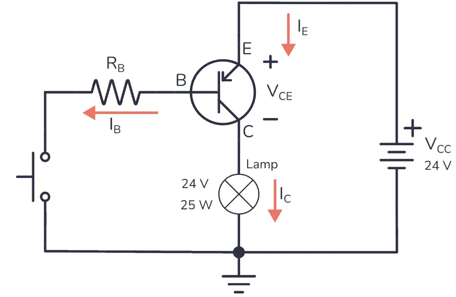
Transistors, when employed as electronic switches, provide a fundamental mechanism for controlling current flow within circuits. This functionality is crucial for countless electronic devices, allowing for the precise activation or deactivation of circuit sections. Understanding this application is key to comprehending broader electronic circuit design.
The basic premise of using a transistor as a switch relies on applying a small current or voltage to its base, which consequently controls a significantly larger current flow between the collector and emitter. This behavior allows for low-power signals to operate higher-power loads, mimicking the function of a mechanical switch but with electronic control and significantly faster switching speeds.
| Component | Function in Switching Circuit |
|---|---|
| Transistor | Acts as the electronic switch, controlling current flow. |
| Base Resistor | Limits the current flowing into the transistor's base. |
| Load Resistor | Defines the electrical load the switch is controlling. |
| Control Signal | Provides the base current to enable switching. |
Consider a simple circuit where an LED is connected as the load between the collector and the positive terminal of the power supply and the emitter is connected to the negative terminal. A resistor connected between the base and the control signal is used to limit the current to the base. When a small control signal is applied, the LED turns on. When the control signal is removed the LED turns off, demonstrating the transistor's function as an effective switch.
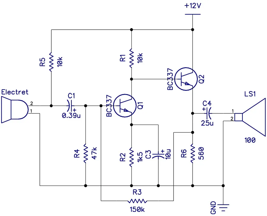
Transistors are not just switches; they are also fundamental building blocks for amplification in electronic circuits. In amplifier applications, a small input signal, such as a voltage or current, is used to control a much larger output signal, effectively boosting the power or magnitude of the signal. This section delves into the mechanics of this process and explores various practical applications where transistors function as amplifiers, complete with illustrative circuit schematics.
At the heart of transistor amplification lies the concept of current control. In a bipolar junction transistor (BJT), a small current applied to the base terminal modulates a larger current flow between the collector and emitter terminals. This current gain, denoted as β (beta), enables the transistor to boost signal amplitude. Similarly, field-effect transistors (FETs) utilize an input voltage at the gate to control the current between the source and drain, allowing voltage amplification.
Understanding the specific circuit configuration is crucial for determining the amplification characteristics. Common amplifier configurations include common-emitter, common-collector, and common-base for BJTs, and common-source, common-gate, and common-drain for FETs. Each configuration exhibits unique properties regarding gain, input impedance, and output impedance, making it suitable for different amplifier applications.
The amplification process also involves biasing the transistor properly. Biasing ensures the transistor operates in the active region, where it can effectively amplify signals without distortion. Proper biasing ensures that the operating point (Q-point) of the transistor is stable and within the desired range for optimal performance. Resistors and other components are often employed to establish these required conditions.
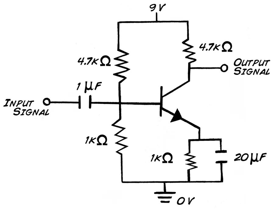
Furthermore, an amplifier is more than just a transistor. In practical amplifier circuits, additional components such as resistors, capacitors, and inductors are included to manage impedance, set the gain, filter out unwanted frequencies, and provide stable feedback paths. An example would be a single-stage audio amplifier schematic, where a transistor is combined with biasing resistors, a coupling capacitor, and a load resistor to boost the audio signal from a source like a microphone.
Here we will consider a practical example for a common-emitter amplifier circuit, which features an NPN transistor, a voltage source (Vcc), base bias resistor (Rb), collector resistor (Rc), and a coupling capacitor (Cc). The input signal is applied through the coupling capacitor to the base of the transistor and the amplified signal output is taken through the collector. When a small varying input signal is applied to the transistor base, this small current variation is amplified, producing a larger variation in current flowing through the transistor, resulting in a higher voltage drop across the collector resistor Rc and this amplified signal is then available at the output. This illustrates the foundational principle of how a transistor can be implemented as a building block for amplification.
These amplification capabilities underpin countless electronic devices. Operational amplifiers (op-amps), which are commonly employed in circuits, utilize multiple transistors in sophisticated configurations to deliver high gain and versatile applications. Transistor amplifiers have a crucial role in everything from simple audio amplification circuits to complex communication systems, and understanding how transistors amplify signals is fundamental to comprehending how those larger circuits function.
This section addresses common queries regarding transistor schematics, providing concise answers to aid understanding. These questions are frequently encountered by those new to electronics and circuit design.
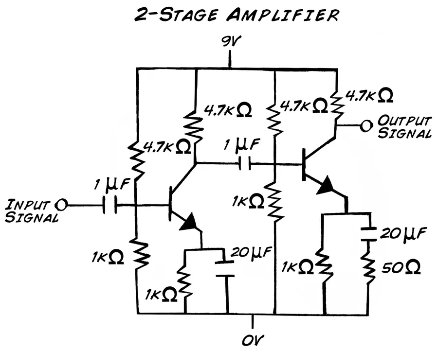
Moving beyond basic single-transistor circuits, advanced transistor schematics explore configurations utilized in more complex systems such as integrated circuits and specialized analog designs. These schematics often incorporate multiple transistors working in concert to achieve specific functions, like signal processing, power regulation, and logic operations. Understanding these configurations is crucial for comprehending modern electronics.
Integrated circuits (ICs), for example, use thousands or even millions of transistors on a single silicon die. While a full IC schematic might be overwhelming to examine, key subsections illustrate how individual transistors combine into complex functional units. Here are some advanced configurations and their purposes:
Analyzing these complex schematics requires a thorough understanding of basic transistor operation and circuit analysis techniques. It is crucial to identify the individual transistor elements and the way they are interconnected to understand a circuit's operation. Below is an example of a schematic diagram that features a complex configuration.
Designing with transistor schematics requires meticulous attention to detail and a solid understanding of both the theoretical underpinnings and practical implications. This section provides key tips to enhance your design process, ensuring accuracy and functionality in your circuits. By focusing on best practices, you can avoid common pitfalls and create robust, reliable designs.
Understanding [transistor schematic] is a core skill in electronics, providing a gateway to designing, building, and repairing complex electronic devices. From basic switches to sophisticated amplifiers, transistors are the building blocks of countless technologies, and mastering their schematic representation empowers anyone to understand how these technologies function and contribute to society. By understanding this visual language, one can delve into the fascinating world of electronics and even innovate new designs.

