In today's world, where technology is rapidly advancing, the humble printed circuit board (PCB) serves as the backbone of countless electronic devices. The process of transforming a design into a physical PCB heavily relies on Gerber files, the lingua franca of PCB manufacturing. These files contain the blueprint needed for fabrication, ensuring that your intricate designs are accurately translated into physical form. This article will dissect Gerber files, exploring their structure, use in PCB production, and how they ensure the fidelity of your designs.
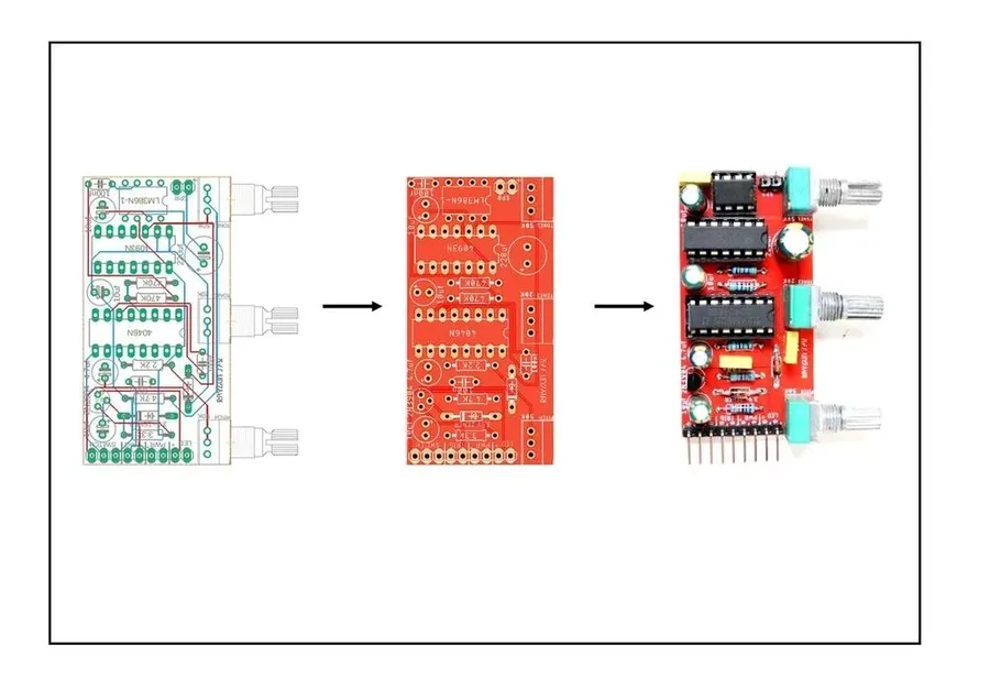
Gerber files are the cornerstone of printed circuit board (PCB) manufacturing. They function as an open ASCII vector format, detailing the precise geometric shapes and features of a PCB design. These files are not merely images; they contain crucial information for every layer of the PCB, ensuring that manufacturers can accurately translate the designer's intent into a physical product. They define the copper traces, pads, vias, solder mask, and silkscreen layers.
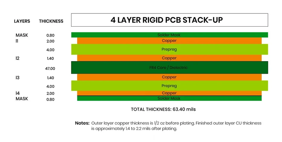
Gerber files, at their core, are meticulously structured to represent the various layers of a Printed Circuit Board (PCB). They utilize a vector-based format, where each layer is described by a series of coordinates and drawing instructions, ensuring accurate reproduction during PCB fabrication. This structure is critical for conveying the precise geometries of copper traces, solder mask openings, silkscreen markings, and other essential board features.
A typical PCB design is composed of multiple layers, each serving a distinct purpose. These layers are individually represented within a set of Gerber files. Understanding these layers is fundamental to interpreting and validating Gerber data.
| Layer Type | Description | Common Gerber Extension |
|---|---|---|
| Copper Layers | Represent conductive paths for electrical signals. PCBs often have multiple copper layers (Top, Bottom, Internal) to facilitate complex routing. | .GTL (Top Copper), .GBL (Bottom Copper), .G1, .G2 (Internal Layers) |
| Solder Mask Layers | Define areas where solder should *not* be applied during assembly, preventing shorts and ensuring reliable connections. Typically a negative image of the copper pads. | .GTS (Top Solder Mask), .GBS (Bottom Solder Mask) |
| Silkscreen Layers | Used for printing component designators, logos, and other informative markings on the PCB. Provides visual aids for assembly and maintenance. | .GTO (Top Silkscreen), .GBO (Bottom Silkscreen) |
| Drill Layer | Specifies the location and size of all holes in the PCB, both plated (vias, component through-holes) and non-plated. | .DRL or .TXT |
| Board Outline | Defines the physical boundaries of the PCB. Often used for panelization and board milling process. | .GKO (Keepout), .GM1 (Mechanical Layer 1) |
The implications of these layers are significant to PCB design. Each layer has its specific requirements and design rules. Incorrect Gerber data for any of these layers can lead to manufacturing errors, functionality issues, or even complete project failure. Therefore, generating and carefully verifying each layer in the Gerber file set is paramount to successful PCB production.
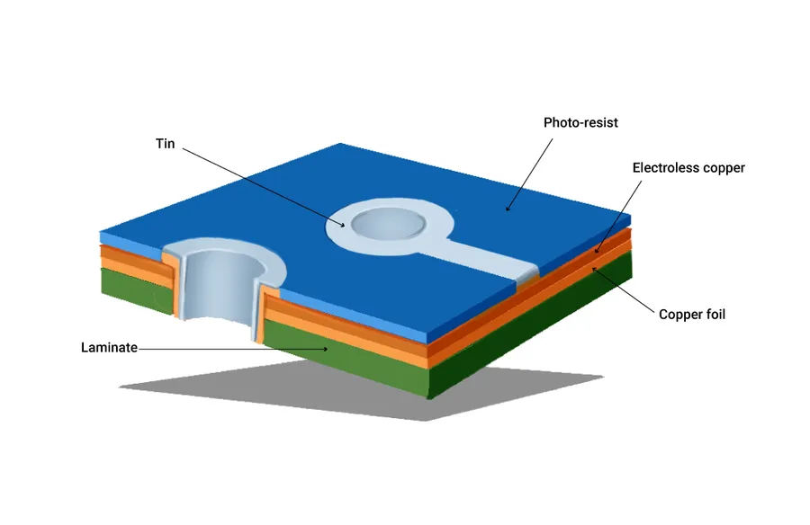
Gerber files are the cornerstone of printed circuit board (PCB) manufacturing, serving as the precise blueprint that guides the fabrication process. These files detail every aspect of the board's design, from the conductive traces to the placement of components, and are crucial for ensuring the accurate and efficient production of PCBs.
The PCB manufacturing process using Gerber files involves a series of critical steps, each requiring precise data interpretation. The process initiates with loading the Gerber data into Computer-Aided Manufacturing (CAM) software at the fabrication facility. This software meticulously interprets the Gerber files, extracting data pertaining to various layers, such as copper traces, solder mask, and silkscreen. Each layer is individually processed and then carefully aligned to form a complete PCB structure. The CAM system generates machine-readable instructions that guide the precision equipment used in PCB fabrication. This includes photoplotters for creating film masks of each layer, drilling machines to create vias and component holes, and etching and plating equipment to develop the conductive patterns on the substrate. Once these individual layers are etched or plated, they are laminated together to form the final structure.
| Manufacturing Step | Description | Gerber File Usage |
|---|---|---|
| Data Loading | Gerber files are imported into CAM software. | File parsing to extract layer data. |
| Panelization | Multiple PCBs are arranged on a single panel for efficient manufacturing. | Gerber data used to generate panel layout. |
| Film Plotting | Photoplots for each layer are created using the Gerber data. | Film is used to transfer patterns onto the PCB material. |
| Drilling | Holes for vias and component leads are drilled. | Drill file information is used to control drill depth and size. |
| Imaging | Copper traces, pads, and other patterns are imaged onto the PCB. | Gerber files guide the exposure process. |
| Etching | Unwanted copper is chemically removed. | Patterns defined in the Gerber data guide the etching process. |
| Solder Mask Application | Solder mask is applied, leaving pads exposed for soldering. | Solder mask layer in Gerber data is used to control solder mask coverage. |
| Silkscreen Printing | Component designators and other text are printed onto the PCB. | Silkscreen layer in Gerber data is used to control text placement. |
| Final Inspection | Completed PCBs are inspected for defects. | Gerber files serve as the reference for the final product. |
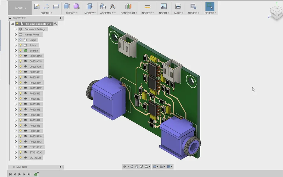
Generating Gerber files is a critical step in the PCB fabrication process, translating your design into a format that manufacturing equipment can understand. This section provides a practical guide on how to generate these files from popular PCB design software, along with essential validation tips to ensure a smooth manufacturing process.
The process generally involves selecting the appropriate output settings within your PCB design software, choosing which layers to export, and verifying the generated files with a Gerber viewer. While the specific steps may vary slightly between different software packages, the underlying principles remain consistent.
Regardless of the software used, ensure that your chosen units (inches or millimeters), the format (RS-274-X is preferred), and layer mapping are configured correctly. Most PCB manufacturers have specific requirements for Gerber files, so refer to their guidelines before exporting.
Following the Gerber file generation process, validation is crucial. This step helps in identifying errors before they make it to the manufacturing stage, preventing costly errors. Here's what to consider:
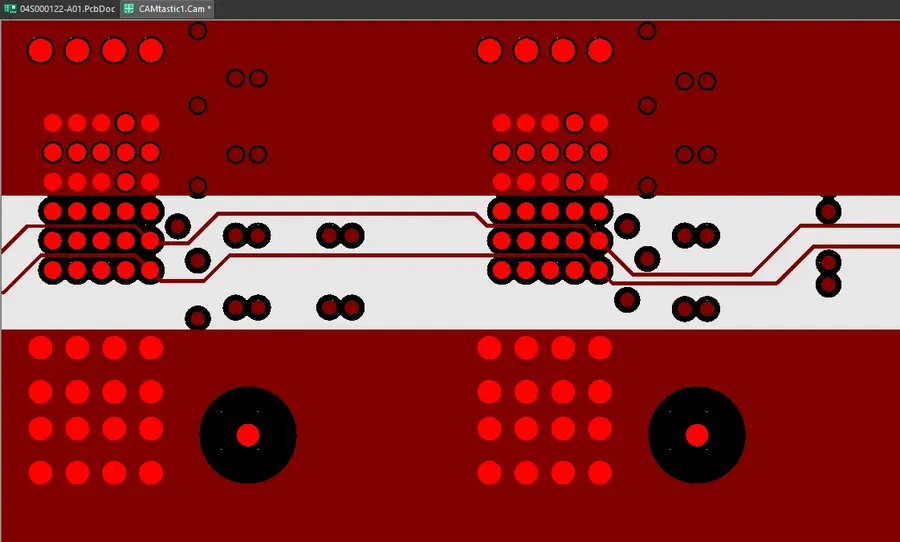
Gerber files, the cornerstone of PCB manufacturing, utilize a variety of file extensions, each denoting a specific layer or aspect of the printed circuit board design. Understanding these extensions is crucial for effective communication between designers and manufacturers.
| File Extension | Description | Common Usage |
|---|---|---|
| .GBR | General Gerber file extension. Often used when the file type is not explicitly defined by another extension. It contains graphical data. | General layer data, may include multiple layers if not specified |
| .GTL | Gerber Top Layer. Represents the top copper layer of the PCB. | Top copper traces, pads and vias |
| .GBL | Gerber Bottom Layer. Corresponds to the bottom copper layer of the PCB. | Bottom copper traces, pads and vias |
| .GTO | Gerber Top Overlay (or Silkscreen). Shows the markings on the top of the PCB. | Component designators, logos, and other silkscreen elements on top layer |
| .GBO | Gerber Bottom Overlay (or Silkscreen). Shows the markings on the bottom of the PCB. | Component designators, logos, and other silkscreen elements on bottom layer |
| .GTS | Gerber Top Solder Mask. Defines the areas where solder should not be applied on the top layer. | Solder mask for top side, protects from solder bridging |
| .GBS | Gerber Bottom Solder Mask. Defines the areas where solder should not be applied on the bottom layer. | Solder mask for bottom side, protects from solder bridging |
| .GKO | Gerber Keep Out Layer. Specifies areas where no components or traces should be placed. | Defines forbidden areas for components, traces, and other conductive parts |
| .DRL | Drill file. Contains the locations and sizes of all drilled holes on the PCB. | Drill hole locations for components, vias and mounting holes |
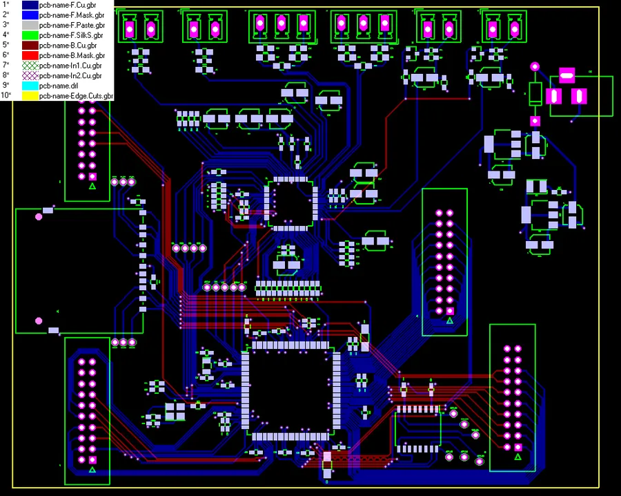
Ensuring Gerber file compatibility and understanding versioning are crucial for successful PCB fabrication. This section explores the different Gerber formats, the importance of compatibility between design software and manufacturing equipment, and the best practices for managing these aspects.
| Feature | RS-274-D | RS-274-X |
|---|---|---|
| Data Format | Basic vector data, requires separate aperture file | Extended Gerber, includes aperture information within the file |
| Aperture Definition | Stored in a separate aperture file (e.g., .APT) | Embedded within the Gerber file |
| Complexity | Simpler format, but requires additional files | More complex, self-contained format |
| Usage | Older format, less common in modern workflows | Modern format, widely adopted for its convenience |
| File Management | Requires managing multiple files, which can lead to errors | Simplifies file management and reduces chances of errors |
The RS-274-X format, also known as Extended Gerber, has largely replaced the older RS-274-D due to its self-contained nature. While RS-274-D requires separate aperture files, the RS-274-X format integrates this data, streamlining the fabrication process. It's important to note that while most modern PCB design software supports both formats, RS-274-X is the generally recommended format for its ease of use and reduced risk of errors.
When working with Gerber files, compatibility between design tools and manufacturing equipment is paramount. Differences in interpretation or software versions can lead to significant issues in the final product. It is vital to generate Gerber files that match the specifications of the PCB manufacturer's equipment and that the manufacturer has a process in place for dealing with version changes to avoid errors and delays. Regularly consult the manufacturer's guidelines to ensure that compatibility requirements are met.
To ensure a smooth manufacturing process, adopt best practices for Gerber file management. Use the latest version of your PCB design software and avoid outdated versions to minimize the risk of compatibility issues. Always perform a thorough validation using Gerber viewers or manufacturer-provided tools before submitting the design. Furthermore, maintain a well-organized file structure to easily track and manage different versions and revisions of Gerber files.
Successfully fabricating a printed circuit board (PCB) hinges on the integrity of the Gerber files. Common issues such as errors and missing data in these files can disrupt the manufacturing process. This section provides troubleshooting guidance to help ensure a smooth transition from design to production.
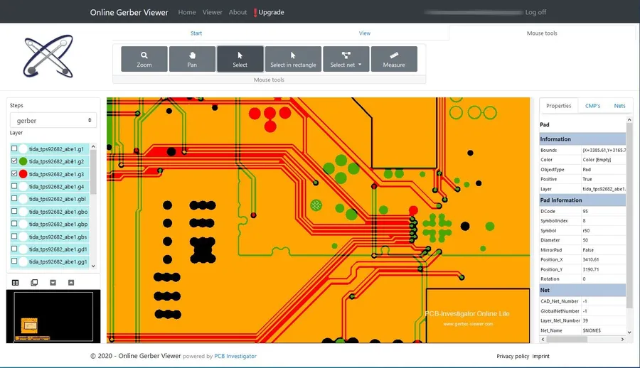
Online Gerber viewers are indispensable tools for PCB designers, offering a convenient way to visually inspect Gerber files before submitting them for manufacturing. These viewers allow for quick validation of the design, ensuring that all layers are correctly aligned and that no critical design elements are missing or misplaced.
By using an online viewer, designers can identify potential issues early in the design process, which can save time and reduce the costs associated with design revisions and manufacturing errors.
These tools typically support standard Gerber formats (RS-274X being most common), allowing a designer to verify the accuracy of their board designs as they will appear to the manufacturer. This capability reduces misunderstandings and improves communication between designers and PCB manufacturers, ultimately leading to a smoother fabrication process.
This section addresses common inquiries regarding Gerber files, providing clear and concise answers to assist with your PCB design and manufacturing process. These questions are derived from common user queries, ensuring they directly address practical concerns.
Gerber files are more than just digital data; they're the bridge connecting PCB design to physical reality. Mastering their intricacies allows designers to ensure precision, quality, and efficiency in PCB fabrication. As technology advances, Gerber files will remain an indispensable part of electronics, guiding the production of the technology we rely on every day. Understanding their nuances empowers you to confidently transform your innovative PCB designs into tangible products.

